GlobalWafers Co (環球晶圓), the world’s third-largest silicon wafer supplier, yesterday said it is to receive US$406 million in subsidies from the US Department of Commerce for two new US fabs under the CHIPS and Science Act, with the first batch of the funds likely coming next year.
The grant represents 10 percent of the planned investments of US$4 billion in advanced semiconductor wafer manufacturing facilities in Texas and Missouri, GlobalWafers said.
The commerce department is to disburse the funds based on the completion of project milestones over a multiyear timeframe, the company said.
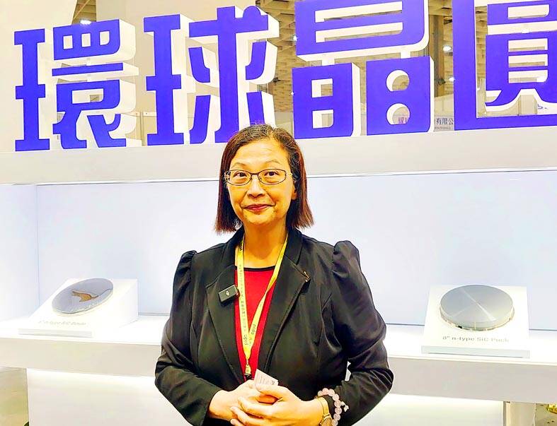
Photo: CNA
Along with the tax credit, which is equal to 25 percent of the qualified investment, the total government funding would make up 35 percent of GlobalWafers’ investments in the US, it said.
The company plans to build a new 12-inch silicon facility in Sherman, Texas, and a new 12-inch silicon on insulator (SOI) wafer plant in St Peters, Missouri, via its subsidiaries GlobalWafers America and MEMC LLC.
GlobalWafers said that it has received orders that would take up 80 percent and 90 percent of the capacities of the Texas and Missouri fabs respectively.
Starting in the first half of next year, GlobalWafers America would become the first high-volume advanced 12-inch silicon wafer facility in the US, the company said.
MEMC is also slated to start manufacture 12-inch silicon-on-insulator wafers in the first half of next year, it added.
“As we plan to achieve the first milestone in the first half of next year, we have an opportunity to receive the first CHIPS Act funding by the end of next year, if everything progresses smoothly,” GlobalWafers chairwoman Doris Hsu (徐秀蘭) told a virtual media briefing yesterday.
The US government funding would “greatly help” mitigate the company’s financial pressure and drive down the depreciation costs of the new facilities and manufacturing equipment, Hsu said.
GlobalWafers is facing mounting financial pressure with its capital expenditures and depreciation costs forecast to peak this year and next year, she said.
The company expects to see a significant improvement in gross margins in 2026 versus next year, as well as a better equipment loading rate and relatively healthier inventory on the semiconductor market, Hsu said.
Amid growing concern that US president-elect Donald Trump could scrap the CHIPS Act when he takes office next month, GlobalWafers said it believes the US government would uphold the law and that no major changes would occur as Washington has a good track record of living up to its promises.
With the new advanced wafer factories in the US, GlobalWafers said it would have a competitive edge over its rivals, given no tariffs, shorter-distance transportation costs and low carbon emissions.
“Our target is to have our wafers certified at all silicon wafer consumers in the US,” Hsu said.
“Starting next year and for the first time in over 20 years, the US will again be home to advanced wafers for leading-edge integrated circuits. Our new facilities will fill a key vulnerability in the US supply chain and bring back to American shores the technology that was pioneered here over 60 years ago,” GlobalWafers president Mark England said in a statement yesterday.
“As the only global wafer manufacturer participating in the CHIPS for America Program, we are fully committed to supporting the nation’s semiconductor manufacturing rebirth,” he said.

Ryanair, Transavia, Volotea and other low-cost airlines are feeling the financial pain from high jet fuel prices as a result of the Middle East war and are cutting flights. The closure of the Strait of Hormuz has taken a huge chunk of oil supplies off the market, sending the price of jet fuel soaring and triggering fears of shortages that could force airlines to cancel flights. Airlines are not waiting for a lack of supplies to react. “Travel alert: Airlines are cutting thousands of flights right now,” Travel Therapy host Karen Schaler said in an Instagram reel this past weekend.

MANAGING RISKS: Taiwan has secured LNG sufficient to cover 95 percent of electricity demand for next month, UBS said, describing the government’s approach as proactive UBS Group AG has raised its forecast for Taiwan’s economic growth this year to 8 percent, up from 6.9 percent previously, and said expansion could reach as high as 8.6 percent if external energy shocks are avoided. The upgrade reflects a stronger-than-expected first-quarter performance and sustained momentum in artificial intelligence (AI)-driven exports, which UBS said are providing a firm foundation for growth despite geopolitical and energy risks. Taiwan’s GDP expanded 13.69 percent year-on-year in the first quarter, the fastest growth since the second quarter of 1987, the Directorate-General of Budget, Accounting and Statistics (DGBAS) reported on Thursday. On a seasonally
The Fair Trade Commission’s (FTC) ongoing review of Grab Holdings Ltd’s US$600 million acquisition of Foodpanda Taiwan’s operations, announced on March 23, has taken on fresh urgency as industry experts warn that the transaction could embed significant Chinese cybersecurity vulnerabilities into Taiwan’s digital infrastructure through Grab’s deep ties to autonomous-driving firm WeRide (文遠知行). Less than 16 months after the FTC blocked Uber Eats’ direct attempt to acquire Foodpanda Taiwan — citing potential combined market shares of 80 to 90 percent — the emergence of Grab as the buyer has prompted questions about whether the same competitive harm is simply being rerouted
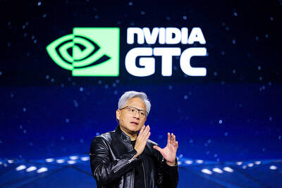
The list of Asian stocks that benefit from business partnership with Nvidia Corp is getting longer, as the region further integrates into the artificial intelligence (AI) chip giant’s business ecosystem. Just in the past week, South Korea’s LG Electronics Inc, Taiwan’s Nanya Technology Corp (南亞科技), as well as China’s Huizhou Desay SV Automotive Co (德賽西威) and Pateo Connect Technology Shanghai Corp (博泰車聯) have become the latest to rally on news of tie-ups, supply-chain participation or product collaboration with the US chip designer. Asian suppliers account for about 90 percent of Nvidia’s production costs, up from about 65 percent last year, data compiled