Developing a localized supply chain for advanced packaging equipment is critical for keeping pace with customers’ increasingly shrinking time-to-market cycles for new artificial intelligence (AI) chips, Taiwan Semiconductor Manufacturing Co (TSMC, 台積電) said yesterday.
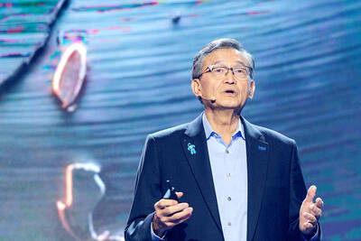
Spurred on by the AI revolution, customers are accelerating product upgrades to nearly every year, compared with the two to three-year development cadence in the past, TSMC vice president of advanced packaging technology and service Jun He (何軍) said at a 3D IC Global Summit organized by SEMI in Taipei.
These shortened cycles put heavy pressure on chipmakers, as the entire process — from chip design to mass production — must now be condensed into a single year, He said.
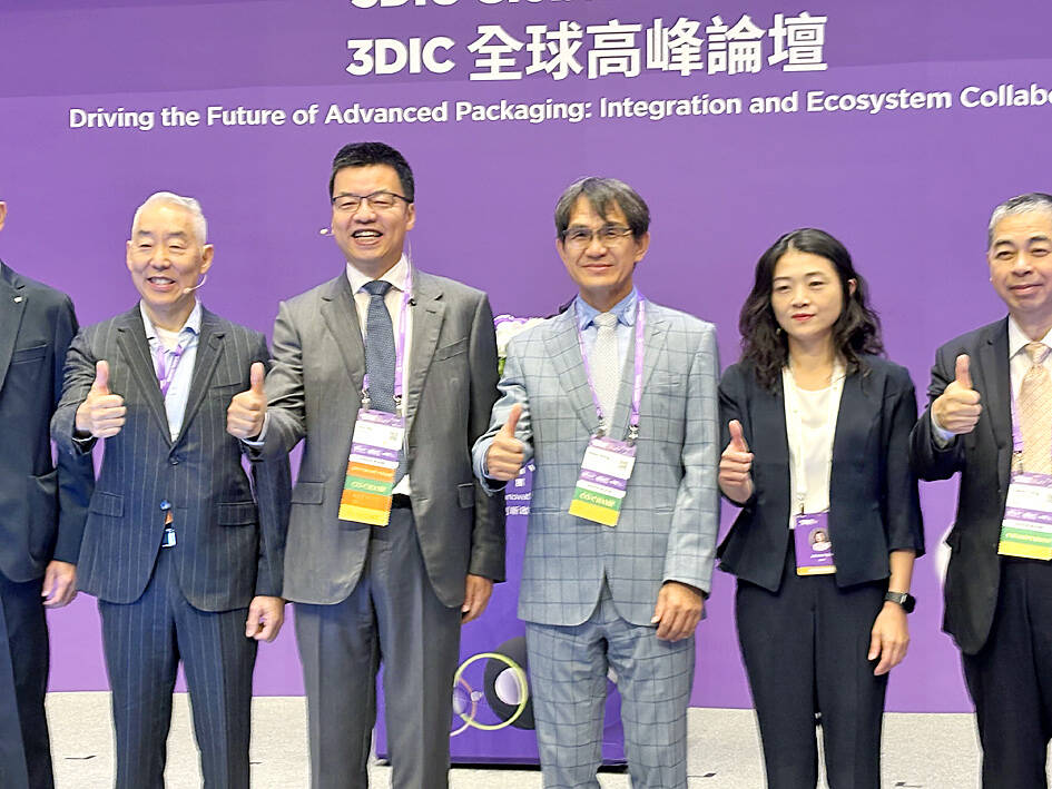
Photo: Grace Hung, Taipei Times
That requires TSMC to ramp up production from zero to peak levels in just three quarters, a 30 percent reduction in the time needed to reach high-volume manufacturing, He said, citing the company’s experience over the past three years producing AI chips using its chip-on-wafer-on-substrate (CoWoS) advanced packaging technology.
TSMC must also maintain yield rates of more than 90 percent to avoid financial losses, since the growing integration of components onto a single chip means even minor defects can result in significant value losses, He said.
TSMC consumes about 10 million high-bandwidth memory (HBM) chips each quarter, He said, citing their central role in AI chip production.
To meet such challenges, TSMC must work closely with partners in the local ecosystem, he said. That need also motivated the company’s launch of the 3D IC Advanced Manufacturing Alliance, first proposed last year and officially inaugurated yesterday.
In the past, TSMC had to procure and install advanced packaging equipment before new chip designs were finalized, leading to frequent adjustments, he said.
“Under such circumstances, localization becomes critically important,” He said, adding that research and development teams from both local and global suppliers are required to be involved early in the development process alongside TSMC’s production teams.
He said that about half of chip development is completed several months before mass production begins.
“So, a localized ecosystem is of the utmost importance,” he said.
The advanced packaging business is “not for the faint-hearted,” given its combination of high risks and high returns, he added.
The global advanced packaging market is forecast to grow at an annual rate of 12.7 percent, reaching US$79 billion by 2030, up from US$38 billion last year, fueled by surging demand for AI applications, Yole Intelligence forecast.
To meet this demand, TSMC has more than doubled its CoWoS capacity over the past two years. CoWoS technology is used to package AI chips
Local advanced packaging equipment suppliers — including ASE Technology Holding Co (日月光投控), Chroma ATE Inc (致茂), Grand Process Technology Corp (弘塑科技) and C Sun Manufacturing Ltd (志聖) — are among the 37 members of the newly established 3D IC Advanced Manufacturing Alliance.

Taiwanese firms have increased investment in the Philippines in recent years as Manila’s ties with Washington deepen and global supply chains continue to shift away from China, an expert at the Chung-Hua Institution for Economic Research (CIER, 中華經濟研究院) said yesterday. The Philippines had not been among Taiwanese investors’ top choices in Southeast Asia, CIER Taiwan ASEAN Studies Center director Kristy Hsu (徐遵慈) said at a seminar in Taipei. However, Taiwan’s investment in the country has grown significantly since the COVID-19 pandemic, reaching US $257 million last year, a high in recent years, she said. Although Taiwan’s total investment in the Philippines still lags
Intel Corp regards Taiwan Semiconductor Manufacturing Co (TSMC, 台積電) as a longstanding partner, as the US chipmaker would continue outsourcing production of advanced chips to TSMC, Intel chief executive officer Lip-Bu Tan (陳立武) said yesterday. “I don’t look at people as competitors. I look at the collaboration... Nvidia is also, you know, a good friend,” Tan told a news conference following his keynote speech at the Computex trade show in Taipei. “It’s a very trusted partnership for us... We are a big, top customer for them, and we’re going to continue doing that,” he said, referring to TSMC, the world’s largest foundry
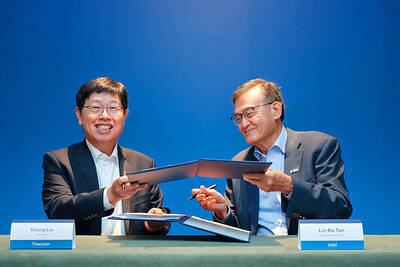
Hon Hai Precision Industry Co (鴻海精密) yesterday said it would work with US chipmaker Intel Corp to jointly develop and deploy next-generation artificial intelligence (AI) infrastructure and intelligent computing platforms in a move to capture booming demand for AI computing systems. Hon Hai, also known as Foxconn Technology Group (富士康), said in a statement that the partnership would combine its global manufacturing scale, system integration expertise and AI data center deployment capabilities with Intel’s strengths in processor architecture, silicon technologies and software ecosystem. The companies said they plan to work on equipment used in AI data centers, including server racks powered by
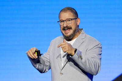
Artificial intelligence (AI) agents would supplant smartphones as the center of people’s digital lives, fundamentally reshaping personal devices and driving a major computing upgrade cycle, Qualcomm Inc CEO Cristiano Amon said yesterday. In his keynote speech for this year’s Computex trade show in Taipei, Amon said that the rise of "agentic AI" — AI systems capable of reasoning, planning and carrying out tasks autonomously — would transform how people interact with technology across phones, PCs, vehicles and wearable devices. Describing the technology as the next major evolution in computing, Amon said that "2026 is the year of agents.” For decades, smartphones have sat