Taiwan Semiconductor Manufacturing Co’s (TSMC, 台積電) board of directors yesterday approved capital appropriations of US$29.62 billion to install and upgrade the firm’s chip manufacturing process technologies, as well as its advanced and mature packaging technology capacity.
The capital expenditure budget would also be for fab construction and installation of manufacturing facilities, the world’s biggest contract chipmaker said in a statement.
TSMC did not comment on reports that it was in talks with flat-panel display maker Innolux Corp (群創) to acquire an idle plant as it prepares to convert manufacturing equipment into a new chip packaging production line that is to use fan-out panel-level packaging (FOPLP) technology.
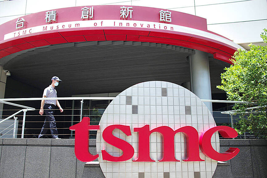
Photo: AFP
Innolux said that about 60 percent of the idle plant’s manufacturing equipment could be reused for the FOPLP technology and its employees have a lot of experience and know-how about glass panel substrates, which are used in panel-level packaging to achieve heterogeneous integration of chips.
TSMC chairman C.C. Wei (魏哲家) last month told investors that the company was “looking at this kind of a panel-level fan-out technology,” as he believed the technology would be mature in about three years.
The chipmaker last month said it planned to spend US$28 billion to US$32 billion this year on new facilities and equipment, with a significant portion earmarked for advanced process technologies such as 2-nanometer technology.
About 10 percent of the capital budget would be for advanced packaging, testing and mask making, it said.
The board in the statement approved a cash dividend of NT$4 per share for the second quarter, as net profit was NT$247.85 billion (US$7.63 billion), or earnings per share of NT$9.56.
The board also gave the go-ahead for a new capital injection of up to US$7.5 billion to TSMC Arizona, a wholly owned subsidiary of TSMC, and the issuance of 2.353 million new “restricted shares” to attract and retain executives and talent, it said.
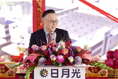
ENERGY ISSUES: The TSIA urged the government to increase natural gas and helium reserves to reduce the impact of the Middle East war on semiconductor supply stability Chip testing and packaging service provider ASE Technology Holding Co (日月光投控) yesterday said it planned to invest more than NT$100 billion (US$3.15 billion) in building a new advanced chip testing facility in Kaohsiung to keep up with customer demand driven by the artificial intelligence (AI) boom. That would be included in the company’s capital expenditure budget next year, ASE said. There is also room to raise this year’s capital spending budget from a record-high US$7 billion estimated three months ago, it added. ASE would have six factories under construction this year, another record-breaking number, ASE chief operating officer Tien Wu

The EU and US are nearing an agreement to coordinate on producing and securing critical minerals, part of a push to break reliance on Chinese supplies. The potential deal would create incentives, such as minimum prices, that could advantage non-Chinese suppliers, according to a draft of an “action plan” seen by Bloomberg. The EU and US would also cooperate on standards, investments and joint projects, as well as coordinate on any supply disruptions by countries like China. The two sides are additionally seeking other “like-minded partners” to join a multicountry accord to help create these new critical mineral supply chains, which feed into

For weeks now, the global tech industry has been waiting for a major artificial intelligence (AI) launch from DeepSeek (深度求索), seen as a benchmark for China’s progress in the fast-moving field. More than a year has passed since the start-up put Chinese AI on the map in early last year with a low-cost chatbot that performed at a similar level to US rivals. However, despite reports and rumors about its imminent release, DeepSeek’s next-generation “V4” model is nowhere in sight. Speculation is also swirling over the geopolitical implications of which computer chips were chosen to train and power the new
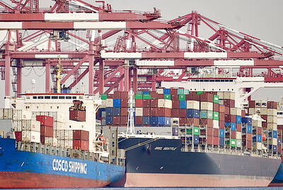
TECH WINNERS: Taiwan and South Korea reported robust trade, which suggests that they have critical advantages in the rapidly expanding AI supply chain, an official said Exports last month surged to a new high, as booming demand tied to artificial intelligence (AI) infrastructure fueled shipments of advanced technology components, underscoring the nation’s pivotal role in the global semiconductor supply chain. Outbound shipments climbed to US$80.18 billion, the highest ever for a single month, rising 61.8 percent from a year earlier and marking the 29th consecutive month of growth, the Ministry of Finance said yesterday. “The surge was driven primarily by global investment in AI infrastructure,” Department of Statistics Director-General Beatrice Tsai (蔡美娜) said. The mass production of next-generation AI computing systems has accelerated procurement across the semiconductor supply