BYD Co (比亞迪), the Chinese automaker backed by Warren Buffett, has come under fire for pollution at one of its factories that residents say has caused nosebleeds in hundreds of children.
Officials in Changsha, the capital of Hunan Province, sent a team to BYD’s factory to investigate gas emissions after receiving complaints from neighbors, the local government said in a statement on its Sina Weibo account on Sunday.
The team includes third-party testing institutions and experts who are to try to get to the bottom of the issue that has seen scores of parents in Changsha protest.
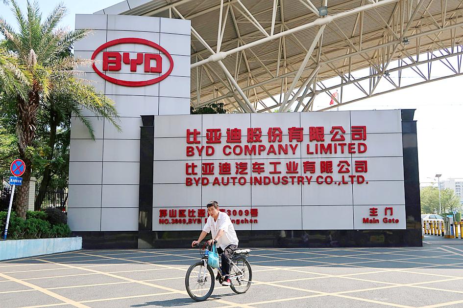
Photo: Reuters
One report said that more than 600 children living near the production plant in the city’s Yuhua District have experienced repeated nosebleeds since last month.
Shenzhen-based BYD said over the weekend that its emissions comply with regulations, adding that it has taken steps to reduce the odor caused by the plant, which has been in operation since 2012.
BYD also said that it has filed police reports alleging the complaints about nosebleeds are groundless and malicious.
The company’s China-traded shares yesterday dropped, falling as much as 4.6 percent, their biggest intraday decline in almost two weeks. Markets in Hong Kong, where BYD is also listed, are closed for a public holiday.
The stock, along with battery maker Contemporary Amperex Technology Co (新能源科技), was among the biggest drags on the CSI 300 index.
BYD is one of China’s most successful vehicle companies in terms of sales, producing both conventional gas automobiles as well as electric vehicles, for which it also makes batteries.
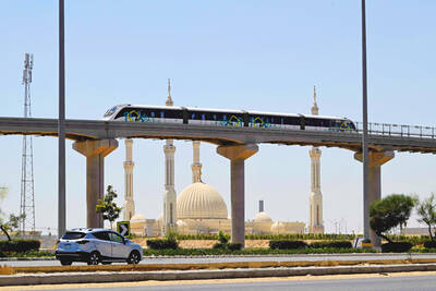
Cairo’s new monorail slices across the city skyline, running above the familiar chaos of blaring horns and aging buses’ exhaust fumes that mark rush hour below. The US$4.5 billion monorail, opened this month, is among Egypt’s most prominent new transport projects, part of a debt-funded infrastructure drive criticized for sapping state finances while bringing limited benefits to most of the country’s 109 million people. “It feels like you’re in a different country,” said Ramy Sayed, a restaurant manager, aboard a driverless Innovia 300 train. “No noise, no traffic, we’re not used to this.” The eastern line runs 56km from the bustling middle-class
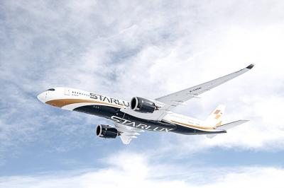
Starlux Airlines Co (星宇航空) today unveiled a long-haul network expansion plan at a shareholders’ meeting in Taipei, including direct flights to Barcelona, Spain, and Zurich, Switzerland, as well as a service connecting Taipei, Sydney and New Zealand. Starlux is to become the first Taiwanese carrier to offer non-stop services to the two European cities, while the inaugural oceanic route is expected to expand transit opportunities within the Australia-New Zealand market, Starlux said. Flight services to Chicago, Dallas, Washington and New York are under evaluation, the airline added. Prior to the shareholders’ meeting, the airline earlier this year announced that it would be

Taiwanese prosecutors suspect that three people successfully smuggled at least one shipment of Nvidia Corp artificial intelligence (AI) chips to China after first exporting them to Japan, people familiar with the matter said. The trio was detained last week by the Keelung District Prosecutors’ Office for allegedly falsifying documents related to exports of Super Micro Computer Inc servers containing advanced Nvidia chips, which the US has barred from sale to China without a license from Washington. The move marked Taiwan’s first public crackdown on AI chip diversion after years of pressure from the US to take a more active role in curtailing
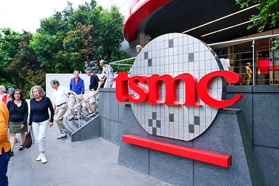
Taiwan Semiconductor Manufacturing Co (TSMC, 台積電) employee bonuses are likely to grow more than 30 percent this year, in line with the past few years as the company’s profits continue to set new records, an anonymous source cited TSMC chairman C.C. Wei (魏哲家) as saying yesterday. TSMC, the world’s largest contract chipmaker, is committed to taking care of its workers, the source said, citing Wei’s meeting with employees yesterday morning. Wei also expressed gratitude to employees for their contribution to the company’s improving bottom line, the source added. Since 2023, TSMC’s employee bonuses have grown at an annual rate of