Hon Hai Precision Industry Co (
The center will focus on nanotechnology and precision-optical machinery.
"We hope the establishment of the new R&D center will expedite our R&D process and, therefore, enhance our competitiveness," Hon Hai's founder and chairman Terry Gou (
Hon Hai, which might replace Singapore's Flextronics International Ltd to become the world's largest EMS provider, plans to expand its R&D manpower to a maximum of 3,000 people and pour NT$12 billion into the center for the next three years.
The company has lodged up to 17,000 applications for patents and has patented around 12,000 inventions so far, Gou said.
The center is expected to facilitate the company's transformation into "high-tech Hon Hai" from merely "manufacturer Hon Hai" by attracting overseas researchers and cooperating with foreign R&D centers, Gou said.
The project has three stages. Hon Hai plans to complete the first-stage of construction by next July and recruit 1,000 R&D specialists at the same time.
The company posted consolidated revenue of NT$327.79 billion last year, up from NT$245.09 billion in 2002. It has generated sales of NT$166.05 billion for the first half of this year, around 37.74 percent of the forecasted NT$440 billion worth of revenue for this year.
"The company often sets aside 10 percent to 15 percent of its annual revenue for the R&D work," said Chen Ga-lane (
Strong R&D capability would back up the company's plan to expand its layouts of computer, communication, consumer electronics (3Cs) into 6Cs domains (3Cs plus cars, channels and [digital] contents), he said.
According to Chen, R&D work in the new center will begin in two years on nanotech stampers, nanotech optics and nanotech heat conductivity, in collaboration with the National Nano Devices Laboratories under the National Science Commission and Tsinghua University in Beijing.
These technologies could be applied in the manufacture of component parts such as nanotech batteries for notebooks or hand-sets, which have double the energy capacity of current batteries, and printer-reader heads for better printing quality, he said.
Hon Hai has set up several R&D centers, including one in Tokyo for precision machinery, Beijing for academic nanotech research, San Jose, California, for e-papers and Finland for wireless technology.
The company's Beijing center is focusing on developing nanotechnology for electronic circuits and devices from single atoms and molecules, but will turn its focus toward miniature batteries and heat-dissipation products within three years, according to a report in a Chinese-language newspaper yesterday.
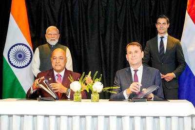
NEW MARKET: The partnership opens up India to the Dutch company, which already has a strong hold in the semiconductor market of South Korea, Taiwan and China ASML Holding NV entered into a partnership agreement with Tata Electronics Pvt Ltd aimed at ramping up India’s goal to develop domestic chip-manufacturing capabilities. The Dutch company’s technology would help power Tata Electronics’ planned 300 millimeter (mm) semiconductor foundry in Gujarat, according to a joint statement from the two companies on Saturday. The signing of a memorandum of understanding coincides with a visit by Indian Prime Minister Narendra Modi to the Netherlands, which is looking to deepen bilateral relations with New Delhi. ASML, whose top customers include Taiwan Semiconductor Manufacturing Co (台積電) and Samsung Electronics Co, makes lithography machines that can print
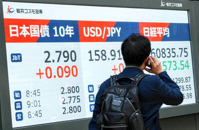
ROUGH RECORDS: Bonds in Japan, as well is in New Zealand, Australia and the US, are seeing the effects of a nervy market as stock exchanges across Asia edge down A deepening slump in Japanese government bonds added fuel to the selloff in global debt markets as rising oil prices stoked inflation fears and pushed yields to multi-decade highs. Japan’s 30-year yield yesterday surged as much as 20 basis points to the highest level since the tenor’s debut in 1999, before paring some of the move. Shorter-maturity Japanese debt was also under pressure, underscored by weak demand at a sale of five-year notes that offered a record-high coupon of 2 percent. Concerns over inflation and government spending rippling through markets including the US, Australia and New Zealand are being amplified in Japan,
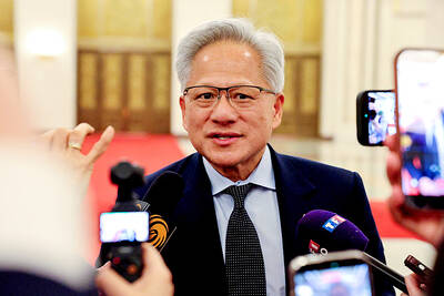
The US has cleared about 10 Chinese firms to buy Nvidia Corp’s second-most powerful artificial intelligence (AI) chip, the H200, but not a single delivery has been made so far, three people familiar with the matter said, leaving a major technology deal in limbo as chief executive officer Jensen Huang (黃仁勳) seeks a breakthrough in China this week. Huang, who was not initially listed in a White House delegation to Beijing, joined the trip after an invitation from US President Donald Trump, a source said. Trump picked him up in Alaska en route to a summit with Chinese President Xi Jinping

Wall Street is licking its chops over an unprecedented slate of massive initial public offerings (IPOs) set to arrive in the coming months, beginning with Elon Musk’s Space Exploration Technologies Corp (SpaceX) next month. That is expected to be followed by artificial intelligence (AI) rivals OpenAI and Anthropic PBC. The trio of mega listings, each eyeing valuations around US$1 trillion or more, constitutes a heady period of elevated risk and reward. SpaceX is targeting an IPO that would raise up to US$80 billion — about double the funds generated from all IPOs last year. OpenAI and Anthropic are eyeing IPOs raising US$60 billion. “We’re