MediaTek Inc (聯發科), the world’s biggest smartphone chip supplier, yesterday said it plans to double investment in data center-related technologies, including advanced packaging and high-speed interconnect technologies, to broaden the new business’ customer and service portfolios.
The chip designer is redirecting its resources to data centers, mainly designing application-specific integrated circuits (ASIC) with artificial intelligence (AI) capabilities for cloud service providers.
The data center business is forecast to lead growth in the next three years and become the company’s second-biggest revenue source, replacing chips used in smart devices, MediaTek president Joe Chen (陳冠州) told a media event in Taipei.
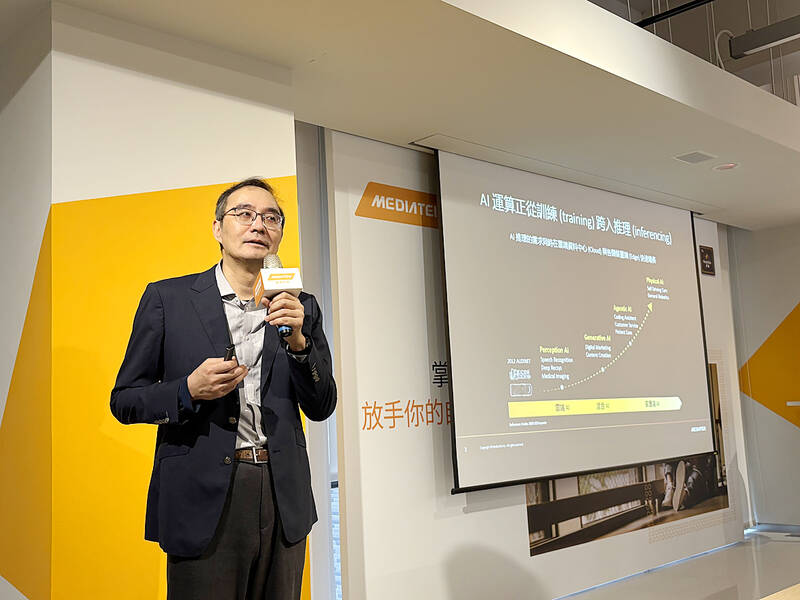
Photo: Lisa Wang, Taipei Times
“Three or four years ago, the [chip] market was driven by consumer [electronics]. Now it is shifting to a high-performance-computing-oriented market either on the cloud or on the edge,” Chen said.
The data center ASIC business would contribute 20 percent to the company’s revenue next year, MediaTek told investors on Wednesday.
To capture new growth opportunities, MediaTek said it plans to invest heavily in critical technologies, to optimize the total ownership of costs of AI data centers by enhancing the computing power of ASIC, Chen said.
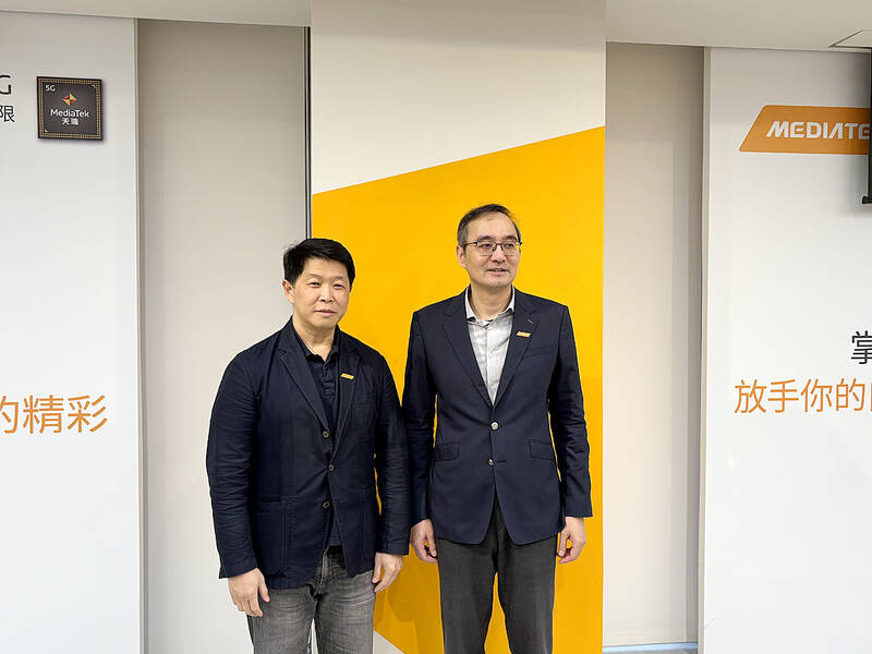
Photo: Lisa Wang, Taipei Times
Toward that end, MediaTek is allocating more resources to develop new advanced packaging technology, co-packaged opticals and silicon photonics technology in collaboration with Taiwan Semiconductor Manufacturing Co (TSMC, 台積電) under the foundry service provider’s compact-universal-photonic-engines platform, to boost energy efficiency and performance, Chen said.
Additionally, the company plans to roll out new high-speed SerDes interface chips later this year with a data operating rate of 400 gigabits per second, double the speed of the previous generation, Chen said.
High-speed SerDes interface technologies are essential for AI, 5G and data center infrastructure to ensure signal integrity.
MediaTek is also pushing for adoption of next-generation chip manufacturing process technologies — 2 nanometers and 14A, or 1.4 nanometers — to enhance the computing power of AI ASIC.
“We will be the first-wave customer of 2-nanometer and A14 advanced process technologies, which will not be limited to data center [chip production],” Chen said.
MediaTek is usually one of the earliest adopters of TSMC’s most advanced processes. TSMC’s 2-nanometer process technology entered volume production late last year and it is expected to start mass production of A14 in 2028.
Asked if MediaTek would consider adopting Intel Corp’s advanced packaging technology, called Embedded Multi-die Interconnect Bridge (EMIB), Chen said the company would be open-minded about it and would see which technology suits its customers best.
Intel’s EMIB technology is considered a potential alternative to TSMC’s chip-on-wafer-on-substrate technology amid severe supply constraints of the advanced packaging technology.

Taiwanese firms have increased investment in the Philippines in recent years as Manila’s ties with Washington deepen and global supply chains continue to shift away from China, an expert at the Chung-Hua Institution for Economic Research (CIER, 中華經濟研究院) said yesterday. The Philippines had not been among Taiwanese investors’ top choices in Southeast Asia, CIER Taiwan ASEAN Studies Center director Kristy Hsu (徐遵慈) said at a seminar in Taipei. However, Taiwan’s investment in the country has grown significantly since the COVID-19 pandemic, reaching US $257 million last year, a high in recent years, she said. Although Taiwan’s total investment in the Philippines still lags
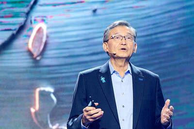
Intel Corp regards Taiwan Semiconductor Manufacturing Co (TSMC, 台積電) as a longstanding partner, as the US chipmaker would continue outsourcing production of advanced chips to TSMC, Intel chief executive officer Lip-Bu Tan (陳立武) said yesterday. “I don’t look at people as competitors. I look at the collaboration... Nvidia is also, you know, a good friend,” Tan told a news conference following his keynote speech at the Computex trade show in Taipei. “It’s a very trusted partnership for us... We are a big, top customer for them, and we’re going to continue doing that,” he said, referring to TSMC, the world’s largest foundry
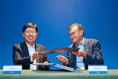
Hon Hai Precision Industry Co (鴻海精密) yesterday said it would work with US chipmaker Intel Corp to jointly develop and deploy next-generation artificial intelligence (AI) infrastructure and intelligent computing platforms in a move to capture booming demand for AI computing systems. Hon Hai, also known as Foxconn Technology Group (富士康), said in a statement that the partnership would combine its global manufacturing scale, system integration expertise and AI data center deployment capabilities with Intel’s strengths in processor architecture, silicon technologies and software ecosystem. The companies said they plan to work on equipment used in AI data centers, including server racks powered by

Artificial intelligence (AI) agents would supplant smartphones as the center of people’s digital lives, fundamentally reshaping personal devices and driving a major computing upgrade cycle, Qualcomm Inc CEO Cristiano Amon said yesterday. In his keynote speech for this year’s Computex trade show in Taipei, Amon said that the rise of "agentic AI" — AI systems capable of reasoning, planning and carrying out tasks autonomously — would transform how people interact with technology across phones, PCs, vehicles and wearable devices. Describing the technology as the next major evolution in computing, Amon said that "2026 is the year of agents.” For decades, smartphones have sat