The US Department of Commerce yesterday said it plans to award SK Hynix Inc up to US$450 million in grants to help fund an advanced packaging plant and research and development (R&D) facility for artificial intelligence (AI) products in Indiana.
In April, SK Hynix, the world’s second-largest memorychip maker, said it would invest about US$3.87 billion to build the facility in West Lafayette, Indiana.
The facility would include an advanced chip production line to mass-produce next-generation high-bandwidth memory chips, currently used in graphic processing units that train AI systems, the Nvidia Corp supplier said.
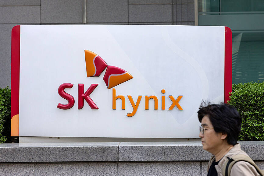
Photo: Bloomberg
The commerce department also plans to make available US$500 million in government loans for the SK Hynix project, which is expected to qualify for a 25 percent investment tax credit.
The memory packaging plant for AI products and an advanced packaging R&D facility would create 1,000 jobs and fill a key gap in the US semiconductor supply chain, the department said.
The US Congress in August 2022 approved a US$39 billion subsidy program for US semiconductor manufacturing and related components along with US$75 billion in government lending authority.
US Secretary of Commerce Gina Raimondo said that the department has announced term sheets with 15 companies offering about US$30 billion in funding that “will unlock another US$300 billion of private capital.”
The US has major commitments from all five major leading-edge semiconductor chip manufacturers — Taiwan Semiconductor Manufacturing Co (台積電), Intel Corp, Samsung Electronics Co, Micron Technology Inc and SK Hynix.
“It means we in the United States will have the most secure and diverse supply chain in the world for the advanced semiconductors that power artificial intelligence,” Raimondo told reporters.
No other economy in the world “has more than two of these companies producing leading-edge chips on its shores,” the department added.
SK Hynix CEO Kwak Noh-jung said in a statement that the company deeply appreciates “the US Department of Commerce’s support and is excited to collaborate in seeing this transformational project fully realized.”
The department in May said it planned to award US$75 million to Absolics Inc for constructing a facility in Georgia to supply advanced materials to the country’s semiconductor industry.
The planned award is to an affiliate of SKC Co, which in turn is part of South Korea’s second-largest conglomerate SK Group, as is SK Hynix.
After several years flying high as Asia’s best Nvidia Corp proxy, Taiwan Semiconductor Manufacturing Co (TSMC, 台積電) is increasingly vying with other artificial intelligence (AI) stocks for investor attention. Stock traders are chasing a wider array of beneficiaries as mainstream usage of AI creates demand for hardware beyond the most-advanced chips TSMC makes for Nvidia. Subthemes from the deepening memory crunch to advances in robotics are also luring bids. At the same time, investment caps on single stocks are pushing funds to diversify, while retail investors long familiar with TSMC through its US depositary receipts are being offered a broader set of
UNDER MICROSCOPE: Taiwan detained three people who allegedly conspired to buy servers in Taiwan and export them using fraudulent documentation, prosecutors said Nvidia Corp chief executive officer Jensen Huang (黃仁勳) on Saturday urged Super Micro Computer Inc to tighten up on compliance after Taiwan detained three people this week for allegedly making fraudulent declarations about artificial intelligence (AI) servers made by its US partner. The development marked the nation’s first crackdown on semiconductor smuggling, which grew after the US slapped restrictions on exports of high-end chips such as Nvidia AI accelerators to China. Nvidia is “rigorous” in explaining regulations to all of its partners, Huang told reporters after arriving in Taipei. “Ultimately Super Micro has to run their own company,” he said in response to

TECH RELIANCE: Growth is increasingly reflecting an unequal K-shaped distribution, where technology sectors outperform and other industries struggle, an expert said Standard Chartered Bank has significantly raised its forecast for Taiwan’s economic growth to 9.5 percent this year, up from 7.6 percent previously, citing surging artificial intelligence (AI) demand driving exports, semiconductor production and investment. The upgrade reflects a sustained AI supercycle that continues to fuel demand for advanced chips and technology infrastructure, which form the backbone of Taiwan’s exports, the bank said in a report this week. “We raise our 2026 growth forecast to reflect a much stronger-than-expected first-quarter GDP figure,” Standard Chartered senior economist for greater China and Asia Tommy Wu (胡東安) said in the report. Driven largely by a 35.3 percent
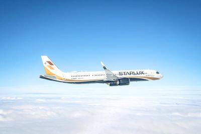
Two of Taiwan’s international carriers, Starlux Airlines Co (星宇航空) and EVA Airways Corp (長榮航空), have retained the five-star airline rating awarded by international airline review organization Skytrax. Starlux was awarded the distinction for a second consecutive year, while EVA Air received it for the 11th straight year, Skytrax said in statements released yesterday and on Thursday last week, respectively. The five-star rating is considered one of the airline industry's highest honors and is awarded following professional audits of airline product and frontline service standards, Skytrax said. The ratings are based on in-depth assessments using unified global quality standards rather than customer review scores