The government is to assist Taiwan Semiconductor Manufacturing Co (TSMC, 台積電) search for a suitable site for an advanced wafer fab, National Development Council (NDC) Minister Kung Ming-hsin (龔明鑫) said yesterday.
Kung’s comments come amid claims from local residents that TSMC has agreed to abandon a planned expansion project in the Longtan (龍潭) section of Hsinchu Science Park (新竹科學園區).
Chinese Nationalist Party (KMT) caucus whip William Tseng (曾銘宗) asked the minister, who sites on TSMC’s board of directors, whether the government — the chipmaker’s single largest investor with a 6.38 percent stake — was aware of the Longtan project.
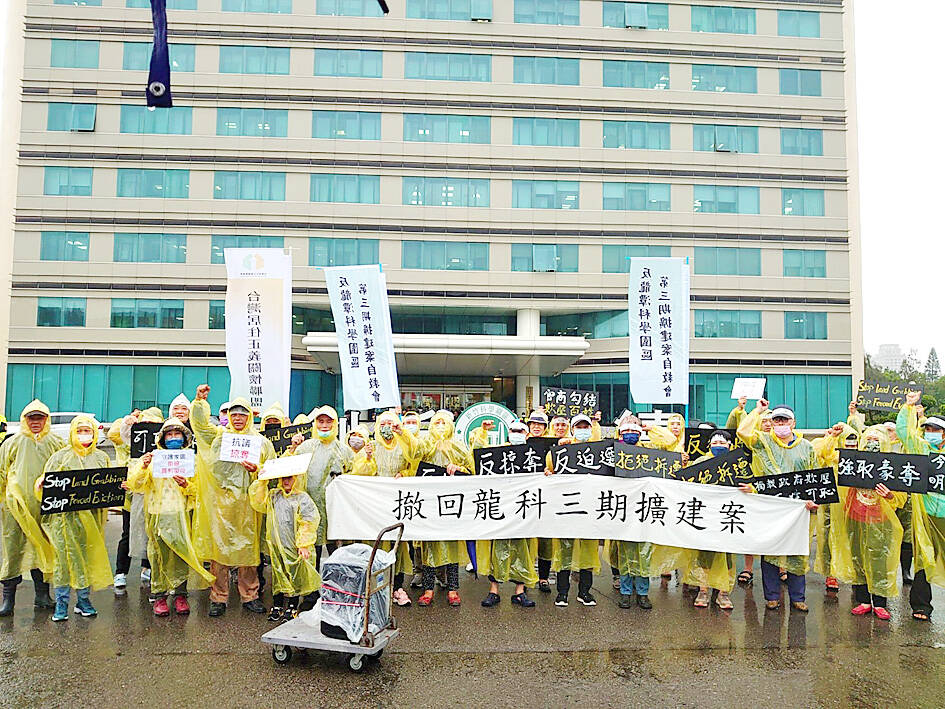
Photo: CNA
Kung said that the government would provide any assistance necessary to help TSMC locate an ideal place in Taichung or Kaohsiung for a wafer fab to make chips with technology more advanced than the 2-nanometer process.
The Hsinchu Science Park Bureau said that the Longtan expansion project covers a 158.59 hectare parcel for semiconductor firms to develop 2-nanometer or more sophisticated technologies.
The project is expected to create 5,900 jobs and generate NT$600 billion to NT$650 billion (US$18.6 billion to US$20.14 billion) in production value per year, it said.
The expansion is aimed at helping upgrade Taiwan’s industrial development, and several semiconductor firms had expressed their willingness to invest in the project, the bureau said.
However, the project has faced strong opposition from Longtan residents on environmental grounds. Several residents staged a protest in front of the bureau on Oct. 4, demanding a withdrawal of the plan.
A group opposed to the expansion wrote on social media that TSMC had expressed a willingness to abandon the project at a meeting with residents and Hsinchu Science Park Bureau representatives.
Kung said that he was not sure whether TSMC had yet proposed leaving the project to its board, while an official from the National Development Fund said the government would stay in contact with the chipmaker on the matter.
TSMC has yet to comment on the claims.
The semiconductor firm started mass production of the advanced 3-nanometer process in Tainan at the end of last year, and is developing the more advanced 2-nanometer process, which is slated to begin commercial production in Hsinchu in 2025, while production is also planned in Kaohsiung.

Taiwanese firms have increased investment in the Philippines in recent years as Manila’s ties with Washington deepen and global supply chains continue to shift away from China, an expert at the Chung-Hua Institution for Economic Research (CIER, 中華經濟研究院) said yesterday. The Philippines had not been among Taiwanese investors’ top choices in Southeast Asia, CIER Taiwan ASEAN Studies Center director Kristy Hsu (徐遵慈) said at a seminar in Taipei. However, Taiwan’s investment in the country has grown significantly since the COVID-19 pandemic, reaching US $257 million last year, a high in recent years, she said. Although Taiwan’s total investment in the Philippines still lags
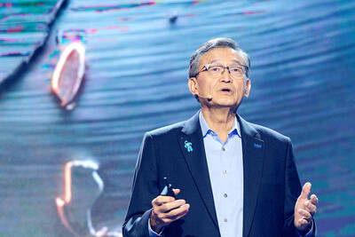
Intel Corp regards Taiwan Semiconductor Manufacturing Co (TSMC, 台積電) as a longstanding partner, as the US chipmaker would continue outsourcing production of advanced chips to TSMC, Intel chief executive officer Lip-Bu Tan (陳立武) said yesterday. “I don’t look at people as competitors. I look at the collaboration... Nvidia is also, you know, a good friend,” Tan told a news conference following his keynote speech at the Computex trade show in Taipei. “It’s a very trusted partnership for us... We are a big, top customer for them, and we’re going to continue doing that,” he said, referring to TSMC, the world’s largest foundry

Artificial intelligence (AI) agents would supplant smartphones as the center of people’s digital lives, fundamentally reshaping personal devices and driving a major computing upgrade cycle, Qualcomm Inc CEO Cristiano Amon said yesterday. In his keynote speech for this year’s Computex trade show in Taipei, Amon said that the rise of "agentic AI" — AI systems capable of reasoning, planning and carrying out tasks autonomously — would transform how people interact with technology across phones, PCs, vehicles and wearable devices. Describing the technology as the next major evolution in computing, Amon said that "2026 is the year of agents.” For decades, smartphones have sat
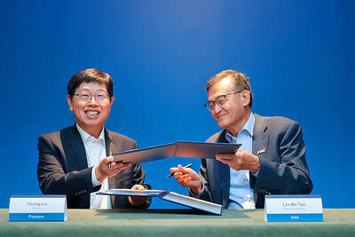
Hon Hai Precision Industry Co (鴻海精密) yesterday said it would work with US chipmaker Intel Corp to jointly develop and deploy next-generation artificial intelligence (AI) infrastructure and intelligent computing platforms in a move to capture booming demand for AI computing systems. Hon Hai, also known as Foxconn Technology Group (富士康), said in a statement that the partnership would combine its global manufacturing scale, system integration expertise and AI data center deployment capabilities with Intel’s strengths in processor architecture, silicon technologies and software ecosystem. The companies said they plan to work on equipment used in AI data centers, including server racks powered by