GlobalWafers Inc (環球晶圓), the world’s No. 3 silicon wafer supplier, yesterday reiterated its positive outlook on business until 2025, as customers continue to show a strong interest in securing wafer supply by signing long-term supply agreements (LTAs).
The Hsinchu-based company saw prepayments from LTAs swell to a record NT$33.11 billion (US$1.12 billion), up 15 percent from the end of last year, undeterred by growing uncertainty about macro environmental risks including impact from COVID-19 lockdowns, the Russia-Ukraine war, rising interest rates, and higher energy and freight costs.
“We continue to sign LTA contracts, especially for larger diameter wafers and advanced products, with 300-millimeter wafers being our customers’ primary target,” GlobalWafers chairperson Doris Hsu (徐秀蘭) told investors at a teleconference.
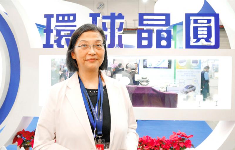
Photo: Fang Wei-jie, Taipei Times
“We have yet to see a cooling-off in demand from our customers,” Hsu said.
“There is some unevenness in the end market, with demand from the smartphone and notebook markets, for example, slowing slightly, while demand from the automotive, industrial and server markets continue to be very hot,” she added.
“So far, there has been no order cancelation or pushout from our customers,” she added.
Demand is strongest for all types of 300-millimeter wafers, followed by wafers made of compound semiconductor materials, mainly silicon carbide and gallium nitride, GlobalWafers said.
To satisfy the robust demand, the company said it was maintaining its NT$100 billion capacity expansion plan, which includes brownfield and greenfield projects at six sites in Taiwan, the US, Italy, South Korea, Japan and Denmark.
Much longer lead times in equipment delivery could create a bottleneck, and that could lead to a delay of one to two quarters in the construction of new production lines, Hsu said.
All production lines are running at full capacity, she said.
In the first quarter, GlobalWafers’ net profit plunged 35 percent year-on-year to NT$1.75 billion, dragged by a loss of more than NT$6 billion from a drop in 13.67 percent-held Siltronic AG’s market value and foreign exchange rate fluctuations.
That translated into earnings per share of NT$4.01, down from NT$6.18 a year earlier.
Excluding the unrealized losses from Siltronic, GlobalWafers would have seen a record profit of NT$14.16 per share last quarter, the company said.
Operating profit surged 49 percent to NT$5.89 billion, and gross margin improved to a record 42.6 percent, from 35.1 percent a year ago.
GlobalWafers said it is hard to predict whether its gross margin would be able to rise to the levels — 46 or 48 percent — posted by foundry companies or integrated device manufacturers, given the uncertainty arising from the impending imposition of a carbon emissions tax and higher energy costs.
Wafer manufacturing is a power-intensive industry, the company said.
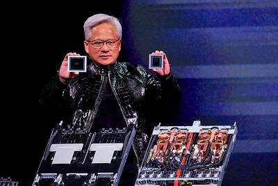
Nvidia Corp chief executive officer Jensen Huang (黃仁勳) on Monday introduced the company’s latest supercomputer platform, featuring six new chips made by Taiwan Semiconductor Manufacturing Co (TSMC, 台積電), saying that it is now “in full production.” “If Vera Rubin is going to be in time for this year, it must be in production by now, and so, today I can tell you that Vera Rubin is in full production,” Huang said during his keynote speech at CES in Las Vegas. The rollout of six concurrent chips for Vera Rubin — the company’s next-generation artificial intelligence (AI) computing platform — marks a strategic

Enhanced tax credits that have helped reduce the cost of health insurance for the vast majority of US Affordable Care Act enrollees expired on Jan.1, cementing higher health costs for millions of Americans at the start of the new year. Democrats forced a 43-day US government shutdown over the issue. Moderate Republicans called for a solution to save their political aspirations this year. US President Donald Trump floated a way out, only to back off after conservative backlash. In the end, no one’s efforts were enough to save the subsidies before their expiration date. A US House of Representatives vote
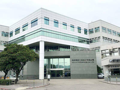
REVENUE PERFORMANCE: Cloud and network products, and electronic components saw strong increases, while smart consumer electronics and computing products fell Hon Hai Precision Industry Co (鴻海精密) yesterday posted 26.51 percent quarterly growth in revenue for last quarter to NT$2.6 trillion (US$82.44 billion), the strongest on record for the period and above expectations, but the company forecast a slight revenue dip this quarter due to seasonal factors. On an annual basis, revenue last quarter grew 22.07 percent, the company said. Analysts on average estimated about NT$2.4 trillion increase. Hon Hai, which assembles servers for Nvidia Corp and iPhones for Apple Inc, is expanding its capacity in the US, adding artificial intelligence (AI) server production in Wisconsin and Texas, where it operates established campuses. This

US President Donald Trump on Friday blocked US photonics firm HieFo Corp’s US$3 million acquisition of assets in New Jersey-based aerospace and defense specialist Emcore Corp, citing national security and China-related concerns. In an order released by the White House, Trump said HieFo was “controlled by a citizen of the People’s Republic of China” and that its 2024 acquisition of Emcore’s businesses led the US president to believe that it might “take action that threatens to impair the national security of the United States.” The order did not name the person or detail Trump’s concerns. “The Transaction is hereby prohibited,”