Efforts to combine nanotechnology with plasma technology have significantly improved due to new equipment which can produce high-performance carbon nanotubes, the National Science Council said yesterday.
Carbon nanotubes are of intense scientific interest around the world due to their outstanding electrical properties.
These properties make them particularly suitable for building a new generation of flat-screen displays known as field emission displays (FED), council officials said at a press conference.
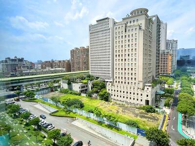
Council Vice Chairman Chi Gou-chung (紀國鐘) said Taiwan might be able to compete with Japan, South Korea and other countries to try to dominate the future FED market with innovative technologies.
Scientists developing the country's first Inductively-Coupled Plasma Chemical Vapor Deposition (ICP-CVD) demonstrated the carbon nanotubes produced in the lab at the press conference.
According to Tsai Chuen-horng (蔡春鴻), a professor of engineering and system science at National Tsing Hua University, the device can produce the kind of high-performance carbon nanotubes needed for the displays.
The technology used in the device has already received two patents from the government and two more from the US.
"With the equipment, we can grow carbon nanotubes homogeneously on a substrate whose diameter is six inches [15.24cm]," Tsai said.
Tsai said this means Taiwanese scientists will be able to develop core technologies for mass production of FED, which could one day replace liquid-crystal displays (LCD).
According to the Industrial Technology Research Institute, this country will become the largest manufacturer of thin-film transistor liquid-crystal displays in the third quarter of this year, taking about 38 percent of the global market.
Over the past four years, Tsai worked with his colleagues and counterparts from National Tai-wan Normal University, Chung Yuan Christian University, the ITRI and Nano Architect Research Corp (晶研科技), studying the growth mechanism of carbon nanotubes, characteristics of field emission and ICP-CVD.
Tsai said the newly-developed equipment might facilitate the production of state-of-the-art, large-scale video display systems.
National Science Council officials told reporters that the NT$38 million research project has resulted in 112 articles for academic journals and conferences.
They said it might possibly produce as many as 12 patents in Taiwan and the US.
Taichung reported the steepest fall in completed home prices among the six special municipalities in the first quarter of this year, data compiled by Taiwan Realty Co (台灣房屋) showed yesterday. From January through last month, the average transaction price for completed homes in Taichung fell 8 percent from a year earlier to NT$299,000 (US$9,483) per ping (3.3m²), said Taiwan Realty, which compiled the data based on the government’s price registration platform. The decline could be attributed to many home buyers choosing relatively affordable used homes to live in themselves, instead of newly built homes in the city’s prime property market, Taiwan Realty

The government yesterday approved applications by Alphabet Inc’s Google to invest NT$27.08 billion (US$859.98 million) in Taiwan, the Ministry of Economic Affairs said in a statement. The Department of Investment Review approved two investments proposed by Google, with much of the funds to be used for data processing and electronic information supply services, as well as inventory procurement businesses in the semiconductor field, the ministry said. It marks the second consecutive year that Google has applied to increase its investment in Taiwan. Google plans to infuse NT$25.34 billion into Charter Investments Ltd (特許投資顧問) through its Singapore-based subsidiary Fructan Holdings Singapore Pte Ltd, and

JET JUICE: The war on Iran’s secondary effects have seen fuel prices skyrocket, knocking flight schedules down to earth in return as airlines struggle with costs Airline passengers should brace for more irritation in the next few months as carriers worldwide cancel flights and ground planes to cope with stratospheric increases in jet-fuel prices. Dutch flag carrier KLM is the latest company to cut its schedule, saying on Thursday that it would scrap 80 return flights at Amsterdam’s Schiphol Airport in the coming month. That puts it in the same league as United Airlines Holdings Inc, Deutsche Lufthansa AG and Cathay Pacific Airways Ltd, which have all pruned itineraries to mitigate costs. Global capacity for next month has been reduced by about 3 percentage points, with all
Micron Technology Inc is a driving force pushing the US Congress to pass legislation that would put new export restrictions on equipment its Chinese competitors use to make their chips, according to people familiar with the matter. A US House of Representatives panel yesterday was to vote on the “MATCH Act,” a bill designed to close gaps in restrictions on chipmaking equipment. It would also pressure foreign companies that sell equipment to Chinese chipmaking facilities to align with export curbs on US companies like Lam Research Corp and Applied Materials Inc. The bill targets facilities operated by China’s ChangXin Memory Technologies Inc