A South Korean executive accused of stealing semiconductor information developed by Samsung Electronics has been detained again on fresh allegations related to the theft of chip processing technology, a court official and his lawyer said yesterday.
The Seoul Central District Court issued a warrant to detain Choi Jinseog on Thursday due to concerns that he was a flight risk, a court official said, who declined to provide further details.
Choi, a former Samsung executive who ran a chipmaking venture in China, has already been the subject of a high-profile industrial espionage trial since July 2023 and was arrested and released on bail last November.

Photo: AFP
Choi has rejected the charges.
He now faces new allegations of being involved in stealing information related to 20-nanometer DRAM chip processing from Samsung, Choi’s lawyer Kim Pilsung said.
Kim said his client denied any wrongdoing and the information he is accused of stealing is publicly available.
Choi has not been indicted over the new allegations, his lawyer said.
Samsung has declined to comment.
In a case that underscores South Korea’s efforts to crack down on industrial espionage and slow China’s progress in chip manufacturing, Choi was indicted in June 2023, accused of seeking to build a copycat chip factory in China with sensitive information developed by Samsung.
The award-winning engineer was once seen as a star in South Korea’s chip industry.
After being freed on bail, Choi said in April that police were investigating him and one of his former employees, an ex-Samsung worker, over fresh allegations related to Samsung’s chip processing technology.

Taichung reported the steepest fall in completed home prices among the six special municipalities in the first quarter of this year, data compiled by Taiwan Realty Co (台灣房屋) showed yesterday. From January through last month, the average transaction price for completed homes in Taichung fell 8 percent from a year earlier to NT$299,000 (US$9,483) per ping (3.3m²), said Taiwan Realty, which compiled the data based on the government’s price registration platform. The decline could be attributed to many home buyers choosing relatively affordable used homes to live in themselves, instead of newly built homes in the city’s prime property market, Taiwan Realty
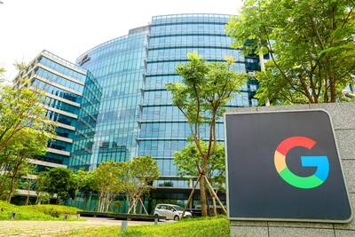
The government yesterday approved applications by Alphabet Inc’s Google to invest NT$27.08 billion (US$859.98 million) in Taiwan, the Ministry of Economic Affairs said in a statement. The Department of Investment Review approved two investments proposed by Google, with much of the funds to be used for data processing and electronic information supply services, as well as inventory procurement businesses in the semiconductor field, the ministry said. It marks the second consecutive year that Google has applied to increase its investment in Taiwan. Google plans to infuse NT$25.34 billion into Charter Investments Ltd (特許投資顧問) through its Singapore-based subsidiary Fructan Holdings Singapore Pte Ltd, and

JET JUICE: The war on Iran’s secondary effects have seen fuel prices skyrocket, knocking flight schedules down to earth in return as airlines struggle with costs Airline passengers should brace for more irritation in the next few months as carriers worldwide cancel flights and ground planes to cope with stratospheric increases in jet-fuel prices. Dutch flag carrier KLM is the latest company to cut its schedule, saying on Thursday that it would scrap 80 return flights at Amsterdam’s Schiphol Airport in the coming month. That puts it in the same league as United Airlines Holdings Inc, Deutsche Lufthansa AG and Cathay Pacific Airways Ltd, which have all pruned itineraries to mitigate costs. Global capacity for next month has been reduced by about 3 percentage points, with all
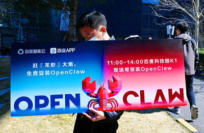
FORESEEABLE CONSEQUENCES: New technology always comes with new innovations by the iniquitous in exploiting users for financial gain or more nefarious ends Artificial intelligence (AI) “agents” say they can save users time and energy by automating tasks, but the growing power of systems such as OpenClaw is putting cybersecurity experts on edge. Powered by a wave of hype, OpenClaw today says it has more than three million users worldwide. The system allows users to create so-called agents, tools based on a large language model (LLM) such as OpenAI’s ChatGPT or Anthropic PBC’s Claude, that can carry out online tasks. “We’ve moved from an AI you could talk with via a chatbot to an agentic AI, which can take action... the threat and the risks are