SK Hynix Inc is ramping up its spending on advanced chip packaging, in hopes of capturing more of the burgeoning demand for a crucial component in artificial intelligence (AI) development: high-bandwidth memory (HBM).
The Icheon-based firm is investing more than US$1 billion in South Korea this year to expand and improve the final steps of its chip manufacture, said Lee Kang-wook, a former Samsung Electronics Co engineer who now heads up packaging development at SK Hynix.
Lee specializes in advanced ways of combining and connecting semiconductors, which has grown in importance with the advent of modern AI and its digestion of vast troves of data via parallel processing chains. While SK Hynix has not disclosed its capital expenditure budget for this year, the average analyst estimate puts the figure at 14 trillion won (US$10.5 billion). That suggests advanced packaging, which could take up a 10th of that, is a major priority.
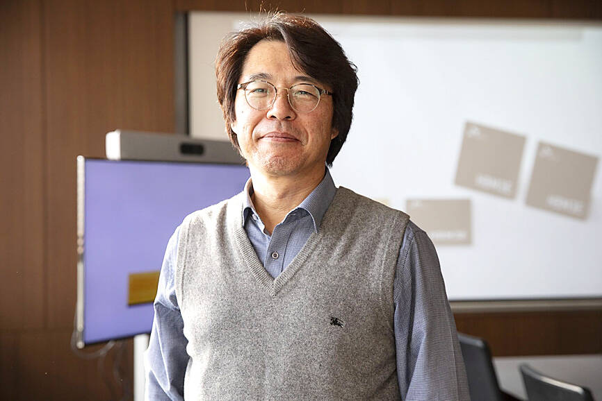
Photo: Bloomberg
“The first 50 years of the semiconductor industry has been about the front-end,” or the design and fabrication of the chips themselves, Lee said in an interview. “But the next 50 years is going to be all about the back-end,” or packaging.
Being first to achieve the next milestone in this race could now catapult companies into industry-leading positions. SK Hynix was chosen by Nvidia Corp to provide the HBM for its standard-setting AI accelerators, pushing the South Korean firm’s value up to 119 trillion won. Its stock gained about 1 percent in Seoul on Thursday, adding to a nearly 120 percent increase since the start of last year. It is now South Korea’s second most valuable company, outperforming Samsung and US rival Micron Technology Inc.
Lee, now 55 years old, helped pioneer a novel method to packaging the third generation of the technology, HBM2E, which was quickly followed by the other two major makers. That innovation was central to SK Hynix winning Nvidia as a customer in late 2019.
HBM is a type of high-performance memory that stacks chips on top of one another and connects them with through-silicon via (TSV) technology for faster and more energy-efficient data processing.
ChatGPT’s release in November 2022 was the moment Lee had been waiting for. By that time, his team had developed a new packaging method called mass reflow-molded underfill (MR-MUF), aided by his contacts in Japan. The process, which involves injecting and then hardening liquid material between layers of silicon, improved heat dissipation and production yields. SK Hynix teamed up with Namics Corp in Japan for the material and a related patent, a person familiar with the matter said.
SK Hynix is pouring the bulk of its new investment into advancing MR-MUF and TSV technologies, Lee said.
Samsung, which has for years been distracted by a succession saga at its very top, is now fighting back. Nvidia last year gave the nod to Samsung’s HBM chips, and the Suwon-based company said on Feb. 26 that it has developed the fifth generation of the technology, HBM3E, with 12 layers of DRAM chips and the industry’s largest capacity of 36 gigabytes.
On the same day, Boise, Idaho-based Micron surprised industry watchers by saying it had begun volume production of 24GB, eight-layer HBM3E, which would be part of Nvidia’s H200 Tensor Core units shipping in the second quarter.
With its big commitment to expanding and enhancing technology at home and a multibillion-dollar advanced packaging facility planned for the US, Lee remains bullish about SK Hynix’s prospects in the face of intensifying competition. He sees the present investment as laying the groundwork to meet more demand to come with future generations of HBM.

Cairo’s new monorail slices across the city skyline, running above the familiar chaos of blaring horns and aging buses’ exhaust fumes that mark rush hour below. The US$4.5 billion monorail, opened this month, is among Egypt’s most prominent new transport projects, part of a debt-funded infrastructure drive criticized for sapping state finances while bringing limited benefits to most of the country’s 109 million people. “It feels like you’re in a different country,” said Ramy Sayed, a restaurant manager, aboard a driverless Innovia 300 train. “No noise, no traffic, we’re not used to this.” The eastern line runs 56km from the bustling middle-class

Taiwanese firms have increased investment in the Philippines in recent years as Manila’s ties with Washington deepen and global supply chains continue to shift away from China, an expert at the Chung-Hua Institution for Economic Research (CIER, 中華經濟研究院) said yesterday. The Philippines had not been among Taiwanese investors’ top choices in Southeast Asia, CIER Taiwan ASEAN Studies Center director Kristy Hsu (徐遵慈) said at a seminar in Taipei. However, Taiwan’s investment in the country has grown significantly since the COVID-19 pandemic, reaching US $257 million last year, a high in recent years, she said. Although Taiwan’s total investment in the Philippines still lags
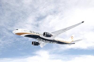
Starlux Airlines Co (星宇航空) today unveiled a long-haul network expansion plan at a shareholders’ meeting in Taipei, including direct flights to Barcelona, Spain, and Zurich, Switzerland, as well as a service connecting Taipei, Sydney and New Zealand. Starlux is to become the first Taiwanese carrier to offer non-stop services to the two European cities, while the inaugural oceanic route is expected to expand transit opportunities within the Australia-New Zealand market, Starlux said. Flight services to Chicago, Dallas, Washington and New York are under evaluation, the airline added. Prior to the shareholders’ meeting, the airline earlier this year announced that it would be
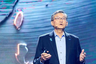
Intel Corp regards Taiwan Semiconductor Manufacturing Co (TSMC, 台積電) as a longstanding partner, as the US chipmaker would continue outsourcing production of advanced chips to TSMC, Intel chief executive officer Lip-Bu Tan (陳立武) said yesterday. “I don’t look at people as competitors. I look at the collaboration... Nvidia is also, you know, a good friend,” Tan told a news conference following his keynote speech at the Computex trade show in Taipei. “It’s a very trusted partnership for us... We are a big, top customer for them, and we’re going to continue doing that,” he said, referring to TSMC, the world’s largest foundry