Taiwan Semiconductor Manufacturing Co (TSMC, 台積電) has secured three construction permits for its plan to build a state-of-the-art A14 wafer fab in Taichung, and is likely to start construction soon, the Central Taiwan Science Park Bureau said yesterday.
Speaking with CNA, Wang Chun-chieh (王俊傑), deputy director general of the science park bureau, said the world’s largest contract chipmaker has received three construction permits — one to build a fab to roll out sophisticated chips, another to build a central utility plant to provide water and electricity for the facility and the other to build three office buildings.
With the three permits, TSMC will be able to begin the construction of its high-speed wafer fab soon, citing a recent briefing to the park authorities by the chipmaker as noting the facility will use the advanced A14 process, Wang said.
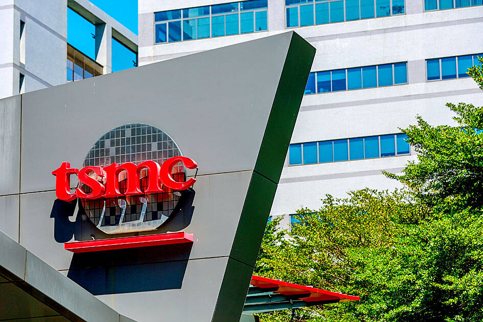
Photo: Ritchie B. Tongo, EPA
Wang’s comments came after the National Science and Technology Council (NSTS) confirmed on Oct. 18 that TSMC had applied for permission from the science authorities to build the A14 fab.
According to information on the TSMC’s Web site, the A14 technology is designed to drive artificial intelligence (AI) transformation by delivering faster computing and greater power efficiency.
The A14 technology, or 1.4-nanometer process, will be 15 percent faster than the 2nm process at the same power, TSMC said. With a 30 percent power reduction, the 1.4nm chip will have the same speed as the 2nm, which is scheduled to start commercial production later this year, the company said.
The 3nm process is the latest technology for which TSMC has started mass production. According to the chipmaker, its advanced processes, including 3nm, 5nm and 7nm, are in high demand during the current AI development boom and the company has intensified efforts to upgrade its technologies to meet growing demand.
The science park has completed preparatory work for the A14 fab site with TSMC conducting join inspections and said the chipmaker is likely to kick off construction work soon.
Taichung City Government has said TSMC’s new fab is expected to create NT$485.7 billion (US$15.85 billion) per year in production value and about 4,500 job openings.
According to the US-based tech site Wccftech, TSMC is aiming to begin construction of the A14 fab at the end of the year and start mass production in the second half of 2028. A recruitment campaign has begun for the new facility, Wccftech said.
To a market estimate, TSMC will spend US$49 billion to build the plant.
Cairo’s new monorail slices across the city skyline, running above the familiar chaos of blaring horns and aging buses’ exhaust fumes that mark rush hour below. The US$4.5 billion monorail, opened this month, is among Egypt’s most prominent new transport projects, part of a debt-funded infrastructure drive criticized for sapping state finances while bringing limited benefits to most of the country’s 109 million people. “It feels like you’re in a different country,” said Ramy Sayed, a restaurant manager, aboard a driverless Innovia 300 train. “No noise, no traffic, we’re not used to this.” The eastern line runs 56km from the bustling middle-class
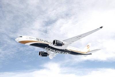
Starlux Airlines Co (星宇航空) today unveiled a long-haul network expansion plan at a shareholders’ meeting in Taipei, including direct flights to Barcelona, Spain, and Zurich, Switzerland, as well as a service connecting Taipei, Sydney and New Zealand. Starlux is to become the first Taiwanese carrier to offer non-stop services to the two European cities, while the inaugural oceanic route is expected to expand transit opportunities within the Australia-New Zealand market, Starlux said. Flight services to Chicago, Dallas, Washington and New York are under evaluation, the airline added. Prior to the shareholders’ meeting, the airline earlier this year announced that it would be
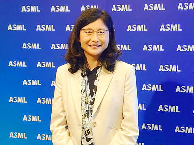
Netherlands-based semiconductor equipment supplier ASML Holding NV yesterday said that it is planning to hire an additional 1,000 people in Taiwan this year in response to growing demand from clients. ASML had previously planned to recruit 600 people this year, but that the plan has been adjusted upward, ASML vice president and ASML Taiwan general manager Grace Wang (汪佳慧) told reporters. ASML has a workforce of more than 4,500 in Taiwan, accounting for about 10 percent of its global total, Wang said. This year’s recruitment campaign would focus on adding people in the customer support, manufacturing and supply chain domains to assist ASML
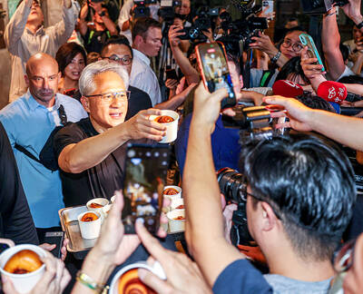
Nvidia Corp yesterday announced that CEO Jensen Huang (黃仁勳) would attend an employee meeting in Taipei tomorrow to celebrate the launch of the company’s Taiwan headquarters project. Huang would attend a gathering at the site of Nvidia’s planned headquarters in Beitou Shilin Technology Park (北投士林科技園區), the company said in a statement. After arriving in Taiwan on Saturday last week, Huang told reporters that he plans to meet with Quanta Computer Inc (廣達) chairman Barry Lam (林百里) and Taiwan Semiconductor Manufacturing Co (TSMC, 台積電) chairman C.C. Wei (魏哲家), and would attend the groundbreaking ceremony for Nvidia’s Taiwan headquarters tomorrow. Nvidia has not yet applied