Government officials and business representatives yesterday participated in a groundbreaking ceremony at the Nanzih Technology Industrial Park (楠梓科技產業園區) in Kaohsiung, where Taiwan Semiconductor Manufacturing Co (TSMC, 台積電) is to construct a 12-inch wafer plant.
The 238-hectare park sits on the former site of a naphtha cracking plant owned by state-owned oil refiner CPC Corp, Taiwan (台灣中油).
Thirty hectares of the first phase of development are reserved for TSMC’s planned factory, while the second phase is to be occupied by international semiconductor material and equipment companies, the Executive Yuan said in a statement yesterday.
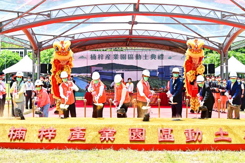
Photo: Ge You-hao, Taipei Times
“The park will be connected with Tainan Science Park (臺南科學園區), Kaohsiung Luzhu Science Park (高雄路竹科學園區) and Kaohsiung Ciaotou Science Park (高雄橋頭科學園區) to form a semiconductor corridor in southern Taiwan, allowing the nation’s technology industry to develop more vigorously,” the statement said.
Kaohsiung Economic Development Bureau Director-General Liao Tai-hsiang (廖泰翔) said the city government has signed a contract with TSMC, with public facilities such as roads and flood detention ponds in the Nanzih park being planned before formal construction.
Liao said construction of the Kaohsiung plant, which the world’s largest contract chipmaker announced in November last year, could start soon.
TSMC has said the plant is to use the advanced 7-nanometer process and the mature 28-nanometer process to produce chips, with production scheduled to begin in 2024.
The city government said earlier that TSMC’s presence in the Nanzih park could help establish a semiconductor cluster in the southern port city within five years, which would boost high-end semiconductor technology development and cultivate a talent pool for the industry.
“Kaohsiung has transformed from an agricultural base into an industrial hub, and the replacement of the CPC’s old naphtha cracking plant by an advanced TSMC fab shows the city is undergoing a rebirth,” Kaohsiung Mayor Chen Chi-mai (陳其邁) said yesterday at the groundbreaking ceremony.
“What people saw first by taking a train to Kaohsiung in the past was CPC’s refinery facilities, but the first stop they will see two years from now will be the TSMC plant,” Chen added.
Addressing the ceremony, Premier Su Tseng-chang (蘇貞昌) said the central government would offer full support to the transformation of Kaohsiung, citing the rapid development of a 5G artificial intelligence of things innovation park in the city’s Asia New Bay Area (亞洲新灣區) over the past year.
Also attending the ceremony yesterday were Minister of Economic Affairs Wang Mei-hua (王美花), Executive Yuan spokesperson Lo Ping-cheng (羅秉成), National Science and Technology Council Minister Wu Tsung-tsong (吳政忠), TSMC vice president for fab operations Wang Ying-lang (王英郎) and CPC chairman Lee Shun-chin (李順欽), as well as representatives from ASML Holding NV, Entegris Inc, Merck Group and Valqua Ltd, the city government said.
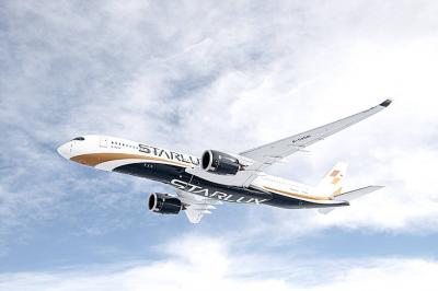
Starlux Airlines Co (星宇航空) today unveiled a long-haul network expansion plan at a shareholders’ meeting in Taipei, including direct flights to Barcelona, Spain, and Zurich, Switzerland, as well as a service connecting Taipei, Sydney and New Zealand. Starlux is to become the first Taiwanese carrier to offer non-stop services to the two European cities, while the inaugural oceanic route is expected to expand transit opportunities within the Australia-New Zealand market, Starlux said. Flight services to Chicago, Dallas, Washington and New York are under evaluation, the airline added. Prior to the shareholders’ meeting, the airline earlier this year announced that it would be
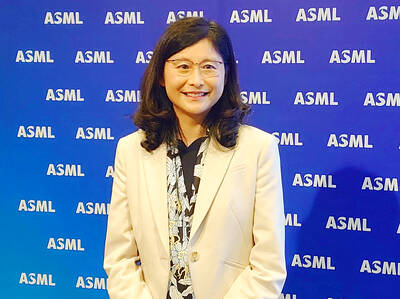
Netherlands-based semiconductor equipment supplier ASML Holding NV yesterday said that it is planning to hire an additional 1,000 people in Taiwan this year in response to growing demand from clients. ASML had previously planned to recruit 600 people this year, but that the plan has been adjusted upward, ASML vice president and ASML Taiwan general manager Grace Wang (汪佳慧) told reporters. ASML has a workforce of more than 4,500 in Taiwan, accounting for about 10 percent of its global total, Wang said. This year’s recruitment campaign would focus on adding people in the customer support, manufacturing and supply chain domains to assist ASML
UNDER MICROSCOPE: Taiwan detained three people who allegedly conspired to buy servers in Taiwan and export them using fraudulent documentation, prosecutors said Nvidia Corp chief executive officer Jensen Huang (黃仁勳) on Saturday urged Super Micro Computer Inc to tighten up on compliance after Taiwan detained three people this week for allegedly making fraudulent declarations about artificial intelligence (AI) servers made by its US partner. The development marked the nation’s first crackdown on semiconductor smuggling, which grew after the US slapped restrictions on exports of high-end chips such as Nvidia AI accelerators to China. Nvidia is “rigorous” in explaining regulations to all of its partners, Huang told reporters after arriving in Taipei. “Ultimately Super Micro has to run their own company,” he said in response to

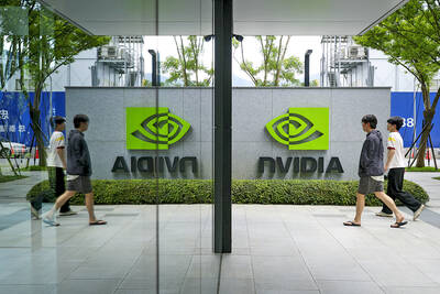
Nvidia Corp yesterday announced that CEO Jensen Huang (黃仁勳) would attend an employee meeting in Taipei tomorrow to celebrate the launch of the company’s Taiwan headquarters project. Huang would attend a gathering at the site of Nvidia’s planned headquarters in Beitou Shilin Technology Park (北投士林科技園區), the company said in a statement. After arriving in Taiwan on Saturday last week, Huang told reporters that he plans to meet with Quanta Computer Inc (廣達) chairman Barry Lam (林百里) and Taiwan Semiconductor Manufacturing Co (TSMC, 台積電) chairman C.C. Wei (魏哲家), and would attend the groundbreaking ceremony for Nvidia’s Taiwan headquarters tomorrow. Nvidia has not yet applied