Intel Corp, the embattled chipmaker now backed by the US government, has introduced new products and manufacturing technology that are central to its turnaround bid.
The company on Thursday announced that its Panther Lake processor designs are in full production and are to go on sale in laptops early next year. The new chips are made with 18A technology, which Intel says offers advantages that none of its competitors can yet match.
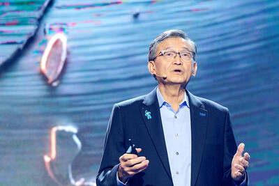
The unveiling follows a furious six-month stretch for Intel chief executive officer Lip-Bu Tan (陳立武). After taking the job in mid-March, he has tried to shake up Intel, while also seeking outside help.
Photo: EPA
The US government has become the chipmaker’s biggest investor as part of an unconventional deal brokered by the White House, while Nvidia Corp and SoftBank Group Corp have acquired multibillion-dollar stakes.
Although the dealmaking has lifted Intel’s stock price, the company still needs to show that new products would win back lost market share and attract customers to its foundry division — a business that makes chips for outside clients.
The Panther Lake design builds on its predecessors’ strengths and eliminates their shortcomings, Intel executives said at a company event in Arizona.
The processors would more readily balance a PC’s need to run demanding software, such as artificial intelligence (AI) models, without rapidly draining batteries.
Intel executives explained the benefits of their latest offerings in presentations hosted near a new factory at its Ocotillo site in Arizona. Known as Fab 52, the facility is the first to go into mass production with the 18A technique.
The once-dominant chipmaker is suffering through its second year of losses, and analysts do not expect a return to profitability before 2027. That slump reflects a dramatic drop in revenue — triggered by market-share declines and a failure to capitalize on surging demand for AI chips in data centers. By getting the jump on Intel in AI, Nvidia has become the industry’s dominant player.
Intel is also shouldering the costly burden of trying to update its factories. Fab 52 alone required more steel than the Eiffel Tower to build and contains machines that cost hundreds of millions of US dollars each.
Over three days of presentations at the event, Intel executives repeatedly asserted that 18A is the most advanced chip production technology developed and deployed in the US. That made-in-the-US spirit lines up with a government push to bolster domestic manufacturing and reduce reliance on factories in East Asia.
The company can make 18A-equipped factories pay for themselves by producing chips for its own needs, Intel said, but the next phase, a technology called 14A, would require outside customers and a high volume of orders to be cost-effective.
Getting the new 18A chips to market, in products that demonstrate better performance for consumers, would be the first step toward re-establishing Intel’s credibility, Intel foundry business general manager Kevin O’Buckley said.

Cairo’s new monorail slices across the city skyline, running above the familiar chaos of blaring horns and aging buses’ exhaust fumes that mark rush hour below. The US$4.5 billion monorail, opened this month, is among Egypt’s most prominent new transport projects, part of a debt-funded infrastructure drive criticized for sapping state finances while bringing limited benefits to most of the country’s 109 million people. “It feels like you’re in a different country,” said Ramy Sayed, a restaurant manager, aboard a driverless Innovia 300 train. “No noise, no traffic, we’re not used to this.” The eastern line runs 56km from the bustling middle-class

Taiwanese firms have increased investment in the Philippines in recent years as Manila’s ties with Washington deepen and global supply chains continue to shift away from China, an expert at the Chung-Hua Institution for Economic Research (CIER, 中華經濟研究院) said yesterday. The Philippines had not been among Taiwanese investors’ top choices in Southeast Asia, CIER Taiwan ASEAN Studies Center director Kristy Hsu (徐遵慈) said at a seminar in Taipei. However, Taiwan’s investment in the country has grown significantly since the COVID-19 pandemic, reaching US $257 million last year, a high in recent years, she said. Although Taiwan’s total investment in the Philippines still lags
Intel Corp regards Taiwan Semiconductor Manufacturing Co (TSMC, 台積電) as a longstanding partner, as the US chipmaker would continue outsourcing production of advanced chips to TSMC, Intel chief executive officer Lip-Bu Tan (陳立武) said yesterday. “I don’t look at people as competitors. I look at the collaboration... Nvidia is also, you know, a good friend,” Tan told a news conference following his keynote speech at the Computex trade show in Taipei. “It’s a very trusted partnership for us... We are a big, top customer for them, and we’re going to continue doing that,” he said, referring to TSMC, the world’s largest foundry

Artificial intelligence (AI) agents would supplant smartphones as the center of people’s digital lives, fundamentally reshaping personal devices and driving a major computing upgrade cycle, Qualcomm Inc CEO Cristiano Amon said yesterday. In his keynote speech for this year’s Computex trade show in Taipei, Amon said that the rise of "agentic AI" — AI systems capable of reasoning, planning and carrying out tasks autonomously — would transform how people interact with technology across phones, PCs, vehicles and wearable devices. Describing the technology as the next major evolution in computing, Amon said that "2026 is the year of agents.” For decades, smartphones have sat