Plasma-based equipment supplier Nano Electronics and Micro System Technologies Inc (暉盛科技) yesterday forecast revenue this year would continue to slip before surging back next year on the back of robust demand for IC substrates for artificial intelligence (AI) applications, and increasing adoption of new glass core substrates and wafer panel-level packaging technology.
The Tainan-based company attributed a slump in its revenue to IC substrate inventory correction over the past two years.
During the first eight months of this year, revenue dropped 7.28 percent to NT$299 million (US$9.8 million), from NT$323 million a year earlier.
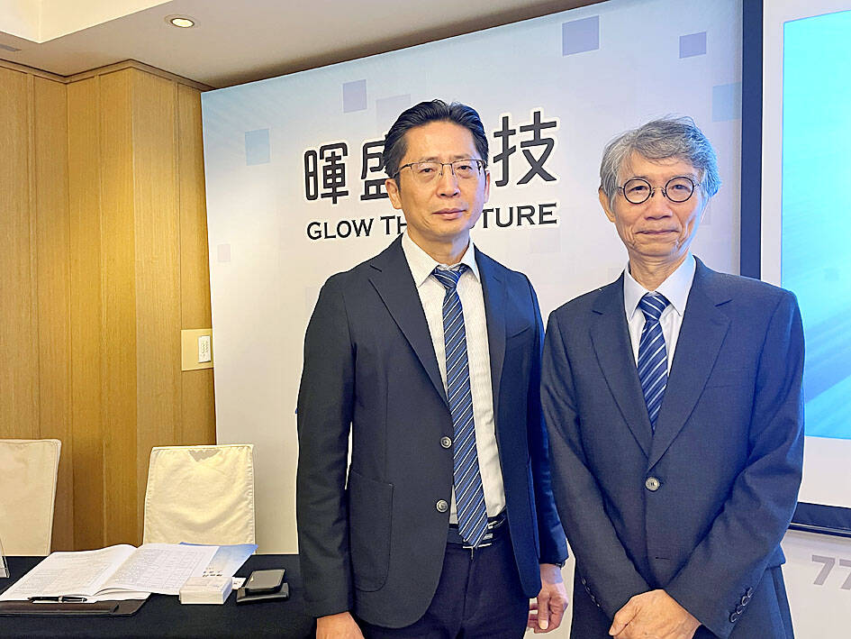
Photo: CNA
The company makes a wide range of equipment for plasma etching, substrate plasma cleaning, de-bond plasma cleaning and wafer plasma etching. The equipment is used by semiconductor, IC substrate and printed circuit board (PCB) makers. Wafer makers, wafer reclaim companies and chip packagers are also among its customers.
“Plasma technology is the core competence of our company. We believe the gold age of plasma is coming,” Nano Electronics chairman Sung Chun-yi (宋俊毅) told a news conference in Taipei.
As OpenAI drives explosive growth for hardware, powered by AI chips, it is critical to raise the yield rate in semiconductor manufacturing, given its high price tag, Sung said.
The company’s plasma equipment could play a key role in improving yield rate, he said.
The company expects the semiconductor segment to become its biggest revenue contributor, making up 46 percent of total revenue next year, up from 17.7 percent this year. The IC substrate segment would fall to the second-largest contributor, accounting for up to 29.4 percent, down from 43.43 percent this year.
“The company’s order visibility is more than six months and could extend to one year,” company spokesman Kelvin Chiu (邱冠陸) said. “In addition, we recently received rush orders from customers from the AI server supply chain, which would help boost revenue growth momentum.”
Next year, the company is looking at new revenue growth from glass core substrate and wafer manufacturing customers as glass core technology is adopted by the whole semiconductor supply chain in preparation for volume production in 2027 or at the beginning of 2028, Chiu said.
It takes up to six months for the company to ship its equipment, he said.
“We are expecting significant growth next year,” he added.
The company counts Taiwan Semiconductor Manufacturing Co (台積電), the world’s biggest contract chipmaker; ASE Technology Holding Co (日月光投控), the world’s biggest chip packager; and PCB suppliers Zhen Ding Technology Holding Ltd (臻鼎) and Unimicron Technology Corp (欣興電子) among its customers.
The company is scheduled to trade its shares on the Taiwan Stock Exchange’s Taiwan Innovation Board next month, becoming the second firm to list on the board this year.
In the first half of this year, the company reported NT$15.15 million in net profit, plunging 62 percent from NT$39.39 million a year earlier, while earnings per share dropped to NT$0.44 from NT$1.14.

Cairo’s new monorail slices across the city skyline, running above the familiar chaos of blaring horns and aging buses’ exhaust fumes that mark rush hour below. The US$4.5 billion monorail, opened this month, is among Egypt’s most prominent new transport projects, part of a debt-funded infrastructure drive criticized for sapping state finances while bringing limited benefits to most of the country’s 109 million people. “It feels like you’re in a different country,” said Ramy Sayed, a restaurant manager, aboard a driverless Innovia 300 train. “No noise, no traffic, we’re not used to this.” The eastern line runs 56km from the bustling middle-class

Taiwanese firms have increased investment in the Philippines in recent years as Manila’s ties with Washington deepen and global supply chains continue to shift away from China, an expert at the Chung-Hua Institution for Economic Research (CIER, 中華經濟研究院) said yesterday. The Philippines had not been among Taiwanese investors’ top choices in Southeast Asia, CIER Taiwan ASEAN Studies Center director Kristy Hsu (徐遵慈) said at a seminar in Taipei. However, Taiwan’s investment in the country has grown significantly since the COVID-19 pandemic, reaching US $257 million last year, a high in recent years, she said. Although Taiwan’s total investment in the Philippines still lags
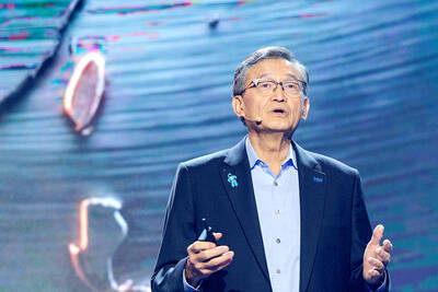
Intel Corp regards Taiwan Semiconductor Manufacturing Co (TSMC, 台積電) as a longstanding partner, as the US chipmaker would continue outsourcing production of advanced chips to TSMC, Intel chief executive officer Lip-Bu Tan (陳立武) said yesterday. “I don’t look at people as competitors. I look at the collaboration... Nvidia is also, you know, a good friend,” Tan told a news conference following his keynote speech at the Computex trade show in Taipei. “It’s a very trusted partnership for us... We are a big, top customer for them, and we’re going to continue doing that,” he said, referring to TSMC, the world’s largest foundry

Artificial intelligence (AI) agents would supplant smartphones as the center of people’s digital lives, fundamentally reshaping personal devices and driving a major computing upgrade cycle, Qualcomm Inc CEO Cristiano Amon said yesterday. In his keynote speech for this year’s Computex trade show in Taipei, Amon said that the rise of "agentic AI" — AI systems capable of reasoning, planning and carrying out tasks autonomously — would transform how people interact with technology across phones, PCs, vehicles and wearable devices. Describing the technology as the next major evolution in computing, Amon said that "2026 is the year of agents.” For decades, smartphones have sat