China has claimed a breakthrough in developing homegrown chipmaking equipment, an important step in overcoming US sanctions designed to thwart Beijing’s semiconductor goals.
State-linked organizations are advised to use a new laser-based immersion lithography machine with a resolution of 65 nanometers or better, the Chinese Ministry of Industry and Information Technology (MIIT) said in an announcement this month.
Although the note does not specify the supplier, the spec marks a significant step up from the previous most advanced indigenous equipment — developed by Shanghai Micro Electronics Equipment Group Co (SMEE, 上海微電子) — which stood at about 90 nanometers.
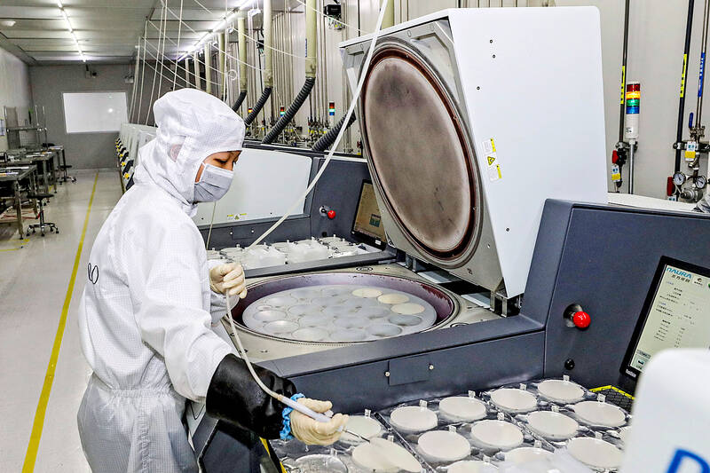
Photo: AFP
MIIT’s claimed advances last week suggest that homegrown Chinese companies are beginning to make headway in developing more sophisticated machines, although SMEE and its peers have a long way to go to catch the likes of ASML Holding NV.
The resolution of the gear determines the scale at which integrated circuits can be imprinted onto silicon, and ASML’s best lithography machines now have a resolution of about 8 nanometers.
One approach to improve the density of transistors is etching lower-resolution patterns multiple times, as used by Huawei Technologies Co (華為), which helps narrow the gap.
Still, the US-led trade campaign to limit China’s access to advanced chipmaking equipment has stifled its competitiveness in developing nascent technologies such as artificial intelligence, which require the most advanced semiconductors.
In its note, the MIIT also named a slew of additional home-developed chip-related gear it wanted to see put into wider use, including oxidation furnaces and dry-etching gear.
SMEE has developed a lithography machine that can be used to make 28-nanometer chips, key state backer Zhangjiang Group (張江集團) declared last year.
However, it is unclear whether that machine has gone into production and how it relates to last week’s notice from the MIIT.
While it is widely believed that China would struggle to move far beyond its current level of sophistication — as exemplified by Huawei’s 7-nanometer Kirin mobile chip introduced a year ago — the lack of transparency has elicited concern in Washington about the effectiveness of its sweeping export controls on China and pressing the Netherlands for tighter restrictions on ASML’s China business.
China relies on ASML’s immersion deep ultraviolet lithography systems to advance its chipmaking technology, as the country has not yet been able to develop similarly capable equipment, but under US pressure, ASML is now barred from shipping to China.

Cairo’s new monorail slices across the city skyline, running above the familiar chaos of blaring horns and aging buses’ exhaust fumes that mark rush hour below. The US$4.5 billion monorail, opened this month, is among Egypt’s most prominent new transport projects, part of a debt-funded infrastructure drive criticized for sapping state finances while bringing limited benefits to most of the country’s 109 million people. “It feels like you’re in a different country,” said Ramy Sayed, a restaurant manager, aboard a driverless Innovia 300 train. “No noise, no traffic, we’re not used to this.” The eastern line runs 56km from the bustling middle-class

Taiwanese firms have increased investment in the Philippines in recent years as Manila’s ties with Washington deepen and global supply chains continue to shift away from China, an expert at the Chung-Hua Institution for Economic Research (CIER, 中華經濟研究院) said yesterday. The Philippines had not been among Taiwanese investors’ top choices in Southeast Asia, CIER Taiwan ASEAN Studies Center director Kristy Hsu (徐遵慈) said at a seminar in Taipei. However, Taiwan’s investment in the country has grown significantly since the COVID-19 pandemic, reaching US $257 million last year, a high in recent years, she said. Although Taiwan’s total investment in the Philippines still lags
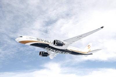
Starlux Airlines Co (星宇航空) today unveiled a long-haul network expansion plan at a shareholders’ meeting in Taipei, including direct flights to Barcelona, Spain, and Zurich, Switzerland, as well as a service connecting Taipei, Sydney and New Zealand. Starlux is to become the first Taiwanese carrier to offer non-stop services to the two European cities, while the inaugural oceanic route is expected to expand transit opportunities within the Australia-New Zealand market, Starlux said. Flight services to Chicago, Dallas, Washington and New York are under evaluation, the airline added. Prior to the shareholders’ meeting, the airline earlier this year announced that it would be
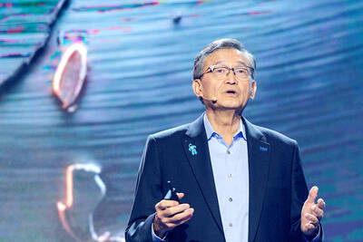
Intel Corp regards Taiwan Semiconductor Manufacturing Co (TSMC, 台積電) as a longstanding partner, as the US chipmaker would continue outsourcing production of advanced chips to TSMC, Intel chief executive officer Lip-Bu Tan (陳立武) said yesterday. “I don’t look at people as competitors. I look at the collaboration... Nvidia is also, you know, a good friend,” Tan told a news conference following his keynote speech at the Computex trade show in Taipei. “It’s a very trusted partnership for us... We are a big, top customer for them, and we’re going to continue doing that,” he said, referring to TSMC, the world’s largest foundry