Taiwan Semiconductor Manufacturing Co (TSMC, 台積電) is expected to move in the first piece of manufacturing equipment for its first 2-nanometer fab in April, paving the way for the world’s biggest contract chipmaker to start producing 2-nanometer chips in 2025, Hsinchu Science Park (新竹科學園區) Bureau director-general Wayne Wang (王永壯) yesterday said.
TSMC’s 2-nanometer fab is in Hsinchu County’s Baoshan Township (寶山), where the science park administration is working on a second-phase development program, after it completes its first-phase program, where it houses TSMC’s new research and development center, Wang said during a ceremony celebrating the science park’s 43rd anniversary.
The infrastructure construction is proceeding smoothly, he said.
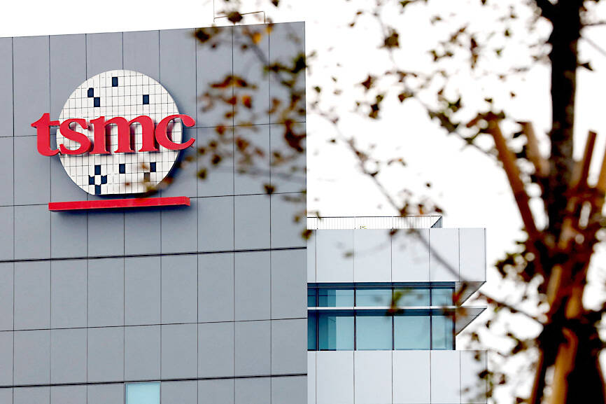
Photo: Reuters, Ann Wang
TSMC’s new 2-nanometer fab construction progress, as Wang described it, indicates that TSMC might be on track to start engineering a pilot run for its 2-nanometer technology next year, before entering a production pilot run and volume production in 2025. The chipmaker said in May that it planned to start building a second 2-nanometer fab next year in Taichung.
However, Taichung Mayor Lu Shiow-yen (盧秀燕) told reporters earlier this week that TSMC could change its mind and consider building a more advanced 1.4-nanometer fab in Taichung, as the chipmaker suffered a setback in securing land to build a 1.4-nanometer fab in the Longtan (龍潭) section of Hsinchu Science Park, amid local protests over government appropriation of privately owned land for industrial use.
TSMC did not comment on whether it has altered its new fab construction plan in Taichung.
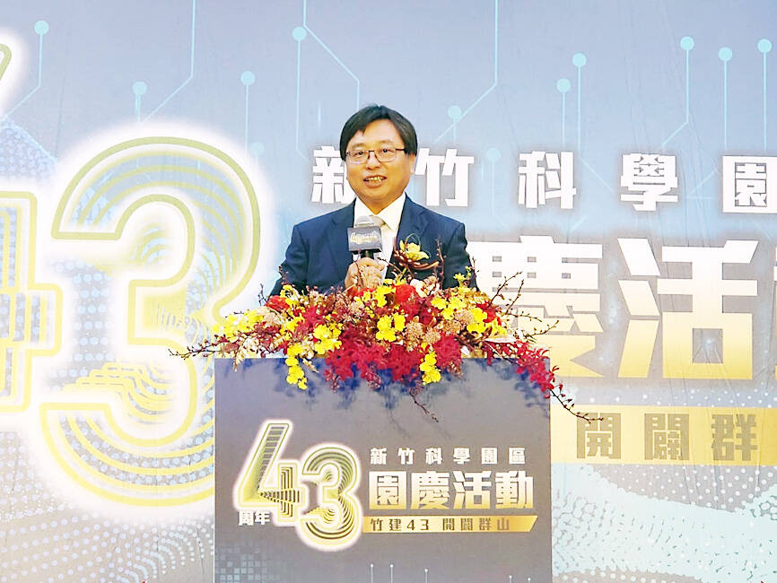
Photo: CNA
Separately, Wang told reporters that the production value of manufacturers in Hsinchu Science Park is set to recover to its peak level starting from next year, following a tough period this year when an economic slowdown and geopolitical tensions cut production value by 19 percent annually in the first half of this year to NT$668.4 billion (US$21.38 billion).
As demand returns, the decline has shrunk to about 10 percent, Wang said. He expects the recovery to extend into 2025, fueling explosive growth in production value to a new record high from companies in the park.
Additionally, the science park bureau said that the third building of the biological technology district within the science park would be completed in the second quarter of next year. It cost more than NT$3 billion, it said.
In addition, the first building of the “X” base is to be completed in the near future, Wang said.
The “X” base is designed to be a hub for the development of emerging technologies such as precision healthcare and generative artificial intelligence.
Poland is betting on a flood of investments and technology transfers from Taiwanese companies to reengineer its US$1 trillion economy. Polish Prime Minister Donald Tusk said yesterday that Poland will no longer be “just an assembly hub” as it pursues further investments from the likes of Foxconn Technology Group (富士康). The firm, whose full name is Hon Hai Precision Industry Co (鴻海精密), last month agreed to build electric vehicles (EVs) in the European Union nation and now could be a partner in a semiconductor venture, he said. The government’s aim is to boost manufacturing and the country’s high-tech chops in an era
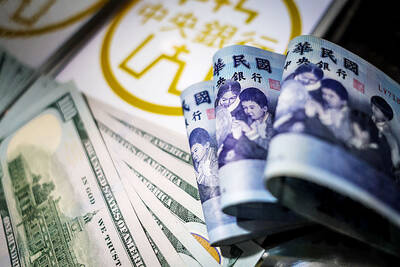
Taiwan remained the sixth-largest net creditor nation in the world last year, despite a fall of more than 10 percent in its net international investment position (NIIP) over the year, the central bank said yesterday. The NIIP is the difference between a country’s external financial assets and its external financial liabilities. Taiwan’s external financial assets hit US$3.27 trillion at the end of last year, up US$275.75 billion or 9.2 percent from a year earlier, the central bank said in its annual NIIP report. The growth largely reflected an increase in holdings of overseas marketable securities by residents in Taiwan, as well as a

RESTRICTION BREACH: ASML said that it denies ‘unfounded rumors regarding non-compliance with export controls concerning China,’ and enforces controls strictly US Secretary of Commerce Howard Lutnick in a series of recent meetings outlined concerns to Dutch chip-equipment giant ASML Holding NV’s senior leaders that one of its top-of-the-line machines might have made its way into China, in violation of US-led export restrictions. In the meetings, Lutnick expressed concern to ASML executives over the company’s extreme ultraviolet lithography (EUV) machines, people familiar with the talks said. EUV systems are used by firms such as Taiwan Semiconductor Manufacturing Co (台積電) to manufacture processors for the likes of Nvidia Corp and Apple Inc. ASML has never been allowed to ship them to China because of curbs
BAD FAITH LITIGATION? The two companies, owned by a California-based private equity firm, could be seeking licensing fees or a settlement payout with the suit Taiwan Intellectual Property Office (TIPO) Director-General Liao Cheng-wei (廖承威) said yesterday he suspected that two firms suing contract chipmaker Taiwan Semiconductor Manufacturing Co (TSMC, 台積電) for patent infringement are “patent trolls.” A patent troll refers to a company that buys patents not for manufacturing products, but to sue other companies for compensation, accusing them of using its patents. Patent trolls, formally called Non-Practicing Entities or Patent Assertion Entities, were responsible for more than 50 percent of lawsuits in the US last year, costing targeted businesses tens of billions of US dollars a year, according to the US-based LegalCharity Web site. Asked whether