NXP Semiconductors NV expects its first automotive-grade 5-nanometer chip built by Taiwan Semiconductor Manufacturing Co (TSMC, 台積電) to become available for automakers within one-and-a-half years at the earliest, following demand for better computing performance and energy efficiency for connected vehicles, a company executive said yesterday.
That would mean a significant upgrade from the 16-nanometer technology NXP adopted in its existing series of microprocessors. NXP chief technology executive Lars Reger made the remarks during a media briefing yesterday in Taipei. The latest updates came after NXP unveiled its plan to source 5-nanometer capacity from TSMC in 2021.
This is Reger’s first trip to Taiwan since the outbreak of the COVID-19 pandemic three years ago. He is slated to pay a visit to TSMC’s Fab 18 in Tainan, the hub for its 5-nanometer chips.
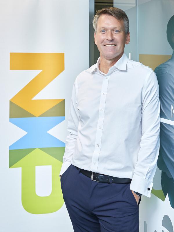
Photo courtesy of NXP Semiconductors NV
“We already gave silicon to our customers as a development platform. The engineering is running,” Reger said. “The new NXP S32 next-generation flagship chip will be available to OEMs in one-and-half to two years and will also be on the mass market.”
With 4 billion transistors on the new 5-nanometer processor, the S32 next-generation flagship chip would deliver optimized network connectivity in real time and enhanced computing and switching performance, Reger said. In the initial stage, no artificial-intelligence (AI) accelerator would be added on, he said.
When asked if NXP would adopt 3-nanometer technology, which has a smaller width between transistors than 5-nanometer chips, Reger said it would largely depend on the benefits brought about. If more AI applications are added on, it would trend smaller, he said.
Beyond Taiwan, NXP is also joining TSMC, Robert Bosch GmbH and Infineon Technologies AG in building a 10 billion euro fab in Dresden, Germany for making car chips in their latest efforts to boost semiconductor supply chain resilience as requested by customers.
TSMC will hold a majority stake of 70 percent in the joint venture. Construction of the fab is to commence in 2027 at the earliest.
NXP customers faced challenges to have sufficient chip supply over the past 3 years due to COVID-19-related restrictions, and have requested to source chips from multiple manufacturing sites or suppliers such as Samsung Electronics Co and GlobalFoundries Inc in different regions, Reger said yesterday.
The strategy of capacity diversification is also extended to chip packaging and development centers, Reger said. This is the “silicon shield” they want to build, he said.
TSMC is building two factories in the US to make advanced 4-nanometer chips used in smartphones and servers for Apple Inc, Nvidia Corp and AMD. The chipmaker also plans to build two factories in Japan to produce chips for Japanese automakers.
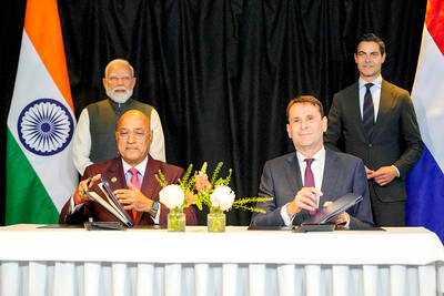
NEW MARKET: The partnership opens up India to the Dutch company, which already has a strong hold in the semiconductor market of South Korea, Taiwan and China ASML Holding NV entered into a partnership agreement with Tata Electronics Pvt Ltd aimed at ramping up India’s goal to develop domestic chip-manufacturing capabilities. The Dutch company’s technology would help power Tata Electronics’ planned 300 millimeter (mm) semiconductor foundry in Gujarat, according to a joint statement from the two companies on Saturday. The signing of a memorandum of understanding coincides with a visit by Indian Prime Minister Narendra Modi to the Netherlands, which is looking to deepen bilateral relations with New Delhi. ASML, whose top customers include Taiwan Semiconductor Manufacturing Co (台積電) and Samsung Electronics Co, makes lithography machines that can print
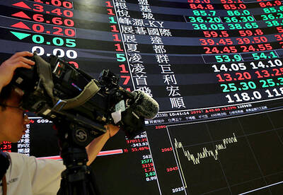
After several years flying high as Asia’s best Nvidia Corp proxy, Taiwan Semiconductor Manufacturing Co (TSMC, 台積電) is increasingly vying with other artificial intelligence (AI) stocks for investor attention. Stock traders are chasing a wider array of beneficiaries as mainstream usage of AI creates demand for hardware beyond the most-advanced chips TSMC makes for Nvidia. Subthemes from the deepening memory crunch to advances in robotics are also luring bids. At the same time, investment caps on single stocks are pushing funds to diversify, while retail investors long familiar with TSMC through its US depositary receipts are being offered a broader set of

TECH RELIANCE: Growth is increasingly reflecting an unequal K-shaped distribution, where technology sectors outperform and other industries struggle, an expert said Standard Chartered Bank has significantly raised its forecast for Taiwan’s economic growth to 9.5 percent this year, up from 7.6 percent previously, citing surging artificial intelligence (AI) demand driving exports, semiconductor production and investment. The upgrade reflects a sustained AI supercycle that continues to fuel demand for advanced chips and technology infrastructure, which form the backbone of Taiwan’s exports, the bank said in a report this week. “We raise our 2026 growth forecast to reflect a much stronger-than-expected first-quarter GDP figure,” Standard Chartered senior economist for greater China and Asia Tommy Wu (胡東安) said in the report. Driven largely by a 35.3 percent
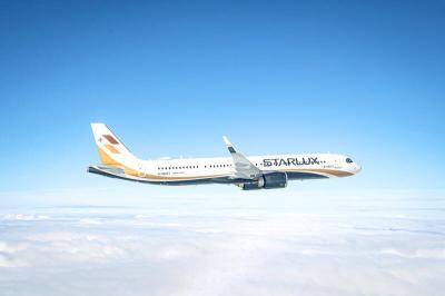
Two of Taiwan’s international carriers, Starlux Airlines Co (星宇航空) and EVA Airways Corp (長榮航空), have retained the five-star airline rating awarded by international airline review organization Skytrax. Starlux was awarded the distinction for a second consecutive year, while EVA Air received it for the 11th straight year, Skytrax said in statements released yesterday and on Thursday last week, respectively. The five-star rating is considered one of the airline industry's highest honors and is awarded following professional audits of airline product and frontline service standards, Skytrax said. The ratings are based on in-depth assessments using unified global quality standards rather than customer review scores