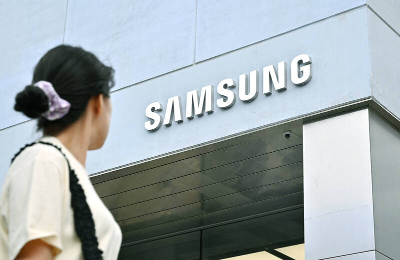
Samsung Electronics Co’s chip foundry business is adding production capacity and more advanced manufacturing techniques, aiming to make gains on market leader Taiwan Semiconductor Manufacturing Co (TSMC, 台積電).
The South Korean company said that it would introduce 2-nanometer production for mobile phone parts by 2025 and expand applications.
Samsung would also significantly increase output in Pyeongtaek, South Korea, and Taylor, Texas, to shore up its foundry division, which makes chips for customers on a contract basis, the company said at a presentation on Tuesday in San Jose, California.

Photo: AFP
The world’s largest memorychip maker is looking to catch up with TSMC while also fending off a nascent challenge from Intel Corp, which is pushing into the foundry market.
While the chip industry in general is suffering from sluggish demand for mobile and personal computer parts, the artificial intelligence boom has spurred interest in advanced processors.
Samsung shared details of its 2-nanometer process technology, which would improve performance by 12 percent and power efficiency by 25 percent compared with its most advanced offering today, which is at 3 nanometers.
Like other chipmakers, Samsung is looking to geographically diversify its manufacturing footprint, which is heavily focused on East Asia.
The company, which has operated a facility in Austin for about 20 years, expects to complete the Taylor plant this year, aiming to commence operations in the second half of next year.
The expansion of production lines at Pyeongtaek along with the Taylor fab would boost Samsung’s capacity sevenfold by 2027 compared with 2021, the company said.
In addition to current chip manufacturing sites, Samsung plans to expand into a new Yongin production base.
US President Joe Biden’s administration is looking to cultivate domestic chip production with about US$50 billion in incentives. US officials have said they would give some of the funds to companies like Samsung and TSMC that are based overseas, but expanding on US soil.
Europe and Japan are also setting aside government money to foster the industry in those locations.
In the US, TSMC is building two fabs in Phoenix, Arizona, at which it is planning to make chips using its advanced 4-nanometer and 3-nanometer processes, with mass production scheduled to begin next year and in 2026 respectively.
The world’s largest contract chipmaker is also building a plant in Japan’s Kumamoto Prefecture, at which its 12-nanometer, 16-nanometer and 22-nanometer processes, as well as 28-nanometer specialty technology, would be used, with commercial production expected to start next year.
Meanwhile, a senior TSMC executive last month said that talks over a possible plant in Germany were continuing and that the earliest a decision would be made is in August.
Additional reporting by CNA and Reuters

Taiwan’s foreign exchange reserves fell below the US$600 billion mark at the end of last month, with the central bank reporting a total of US$596.89 billion — a decline of US$8.6 billion from February — ending a three-month streak of increases. The central bank attributed the drop to a combination of factors such as outflows by foreign institutional investors, currency fluctuations and its own market interventions. “The large-scale outflows disrupted the balance of supply and demand in the foreign exchange market, prompting the central bank to intervene repeatedly by selling US dollars to stabilize the local currency,” Department of Foreign

ENERGY ISSUES: The TSIA urged the government to increase natural gas and helium reserves to reduce the impact of the Middle East war on semiconductor supply stability Chip testing and packaging service provider ASE Technology Holding Co (日月光投控) yesterday said it planned to invest more than NT$100 billion (US$3.15 billion) in building a new advanced chip testing facility in Kaohsiung to keep up with customer demand driven by the artificial intelligence (AI) boom. That would be included in the company’s capital expenditure budget next year, ASE said. There is also room to raise this year’s capital spending budget from a record-high US$7 billion estimated three months ago, it added. ASE would have six factories under construction this year, another record-breaking number, ASE chief operating officer Tien Wu

The EU and US are nearing an agreement to coordinate on producing and securing critical minerals, part of a push to break reliance on Chinese supplies. The potential deal would create incentives, such as minimum prices, that could advantage non-Chinese suppliers, according to a draft of an “action plan” seen by Bloomberg. The EU and US would also cooperate on standards, investments and joint projects, as well as coordinate on any supply disruptions by countries like China. The two sides are additionally seeking other “like-minded partners” to join a multicountry accord to help create these new critical mineral supply chains, which feed into

For weeks now, the global tech industry has been waiting for a major artificial intelligence (AI) launch from DeepSeek (深度求索), seen as a benchmark for China’s progress in the fast-moving field. More than a year has passed since the start-up put Chinese AI on the map in early last year with a low-cost chatbot that performed at a similar level to US rivals. However, despite reports and rumors about its imminent release, DeepSeek’s next-generation “V4” model is nowhere in sight. Speculation is also swirling over the geopolitical implications of which computer chips were chosen to train and power the new