Taiwan Semiconductor Manufacturing Co (TSMC, 台積電) is to build a wafer fab deploying 1 nanometer (nm) process technology at the Longtan (龍潭) campus of Hsinchu Science Park (新竹科學園區), Hsinchu Science Park Bureau Director-General Wayne Wang (王永壯) said yesterday.
The bureau completed a pilot project in the middle of last month for the third expansion phase of the Longtan Science Park (龍潭科學園區) in Taoyuan to accommodate the new TSMC plant, Wang told a news conference.
The pilot expansion project has been submitted to the National Science and Technology Council, which would next forward the project to the Cabinet for approval, Wang said.
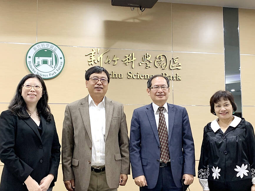
Photo: Grace Hung, Taipei Times
“The efforts by the government to push for the construction of TSMC’s 1-nanometer process fab are proceeding smoothly,” he added.
Local media reports have said that the Longtan park’s third expansion phase would cover 150 hectares.
As 90 percent of the land is privately owned, it would require a huge effort to expropriate the land needed, the reports said.
2-NANOMETER FAB
Meanwhile, a new expansion plan in the Central Taiwan Science Park (中部科學園區) passed its third review yesterday, clearing the way for its final passage during a general review early next year, which would allow TSMC to build a 2-nanometer fab by the middle of next year, the Central Taiwan Science Park Administration said yesterday.
The administration said in a statement that it would submit supplementary information about the second-phase expansion plan to the Environmental Protection Administration as soon as possible after receiving a written record of the review.
The administration aims to complete all administrative procedures and hand over the land to local foundry companies to build new factories by the middle of next year, it said.
It added that it plans to attract other technology firms to set up facilities in the park to support the expansion and development of the semiconductor industry in Taiwan.
The development project would create NT$485.7 billion (US$15.95 billion) in production value a year and 4,500 direct jobs, the statement said.
TSMC plans to start pilot production of 2-nanometer chips in the second half of 2024 and commence mass production in 2025.
Its development of 2-nanometer process technology is progressing well and is even a little ahead of its schedule, TSMC chief executive C.C. Wei (魏哲家) said in October.
Customer engagement with the 2-nanometer chips is comparable with their engagement with the company’s 3-nanometer and 5-nanometer chips, he said.
TSMC said its 2-nanometer technology would be the most advanced in terms of density and energy efficiency when it is introduced.
ARIZONA FAB
The company is scheduled to hold a “first tool-in” ceremony for its new Arizona fab today to mark the installation of the first batch of production equipment, with US President Joe Biden expected to attend the event.
The company is spending US$12 billion to build a 5-nanometer fab in Arizona, with mass production to start in 2024. It plans to introduce 3-nanometer process technology during the second phase of the Arizona investment.

Cairo’s new monorail slices across the city skyline, running above the familiar chaos of blaring horns and aging buses’ exhaust fumes that mark rush hour below. The US$4.5 billion monorail, opened this month, is among Egypt’s most prominent new transport projects, part of a debt-funded infrastructure drive criticized for sapping state finances while bringing limited benefits to most of the country’s 109 million people. “It feels like you’re in a different country,” said Ramy Sayed, a restaurant manager, aboard a driverless Innovia 300 train. “No noise, no traffic, we’re not used to this.” The eastern line runs 56km from the bustling middle-class
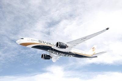
Starlux Airlines Co (星宇航空) today unveiled a long-haul network expansion plan at a shareholders’ meeting in Taipei, including direct flights to Barcelona, Spain, and Zurich, Switzerland, as well as a service connecting Taipei, Sydney and New Zealand. Starlux is to become the first Taiwanese carrier to offer non-stop services to the two European cities, while the inaugural oceanic route is expected to expand transit opportunities within the Australia-New Zealand market, Starlux said. Flight services to Chicago, Dallas, Washington and New York are under evaluation, the airline added. Prior to the shareholders’ meeting, the airline earlier this year announced that it would be
Taiwanese prosecutors suspect that three people successfully smuggled at least one shipment of Nvidia Corp artificial intelligence (AI) chips to China after first exporting them to Japan, people familiar with the matter said. The trio was detained last week by the Keelung District Prosecutors’ Office for allegedly falsifying documents related to exports of Super Micro Computer Inc servers containing advanced Nvidia chips, which the US has barred from sale to China without a license from Washington. The move marked Taiwan’s first public crackdown on AI chip diversion after years of pressure from the US to take a more active role in curtailing
Taiwan Semiconductor Manufacturing Co (TSMC, 台積電) employee bonuses are likely to grow more than 30 percent this year, in line with the past few years as the company’s profits continue to set new records, an anonymous source cited TSMC chairman C.C. Wei (魏哲家) as saying yesterday. TSMC, the world’s largest contract chipmaker, is committed to taking care of its workers, the source said, citing Wei’s meeting with employees yesterday morning. Wei also expressed gratitude to employees for their contribution to the company’s improving bottom line, the source added. Since 2023, TSMC’s employee bonuses have grown at an annual rate of