A joint venture by Hon Hai Precision Industry Co (鴻海精密) and India’s Vedanta Ltd to build a semiconductor plant in Gujarat state, India, could start producing 12-inch wafers using the 28-nanometer process in 2025, a Vedanta executive said on Sunday.
Last month, Indian media reported that the two firms had signed a US$19.5 billion investment pact to set up a semiconductor factory in Gujarat, the home state of Indian Prime Minister Narenda Modi.
Akarsh Hebbar, Vedanta’s global managing director of display and semiconductor business, on Sunday offered new details on what the project would entail.
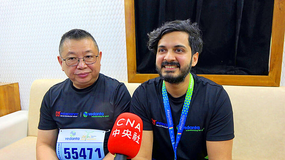
Photo: CNA
The companies are looking at Dholera, where they are close to finalizing a 162-hectare plot for the plant, Hebbar said.
They plan to begin operations at the plant in 2025 or 2026, producing 12-inch wafers based on the 28-nanometer process, which is widely used in appliances, automobiles and mobile phones, he said.
After opening, the facility would take about one year to ramp up production, after which it would be producing about 40,000 wafers per month, mainly for the Indian market, Hebbar said.
He said he was confident that the project would be able to overcome some of the challenges to manufacturing chips in India, such as access to relevant supply chains, and sufficient water and power resources.
Specifically, he cited his own company’s experience with clean room technology, which is required for semiconductor manufacturing, as well as utility guarantees and subsidies that the project has received from the state government.
In terms of supply chains, Hebbar said that the project would bring together an “ecosystem” of more than 100 international subcontractors at the factory, thus enhancing its operational efficiency.
Media reports last month said that Hon Hai, known internationally as Foxconn Technology Group (富士康科技集團), would act as a technical partner, while funding would come mainly from Vedanta, a mining conglomerate that has recently sought to diversify into chip manufacturing.

Taiwan’s foreign exchange reserves fell below the US$600 billion mark at the end of last month, with the central bank reporting a total of US$596.89 billion — a decline of US$8.6 billion from February — ending a three-month streak of increases. The central bank attributed the drop to a combination of factors such as outflows by foreign institutional investors, currency fluctuations and its own market interventions. “The large-scale outflows disrupted the balance of supply and demand in the foreign exchange market, prompting the central bank to intervene repeatedly by selling US dollars to stabilize the local currency,” Department of Foreign

Intel Corp is joining Elon Musk’s long-shot effort to develop semiconductors for Tesla Inc, Space Exploration Technologies Corp and xAI, marking a surprising twist in the chipmaker’s comeback bid. Intel would help the Terafab project “refactor” the technology in a chip factory, the company said on Tuesday in a post on X, Musk’s social media platform. That is a stage in the development process that typically helps make chips more powerful or reliable. The chipmaker’s shares jumped 4.2 percent to US$52.91 in New York trading on Tuesday. The Terafab project is a grand plan by Musk to eventually manufacture his own chips for

Taiwan Power Co (Taipower, 台電) yesterday said it plans to resume operations at two coal-fired power generators for three months to boost security of electricity supply as liquefied natural gas (LNG) supply risks are running high due to the Middle East conflict. The two coal-fired power generators are at Mailiao Power Plant in Yunlin County’s Mailiao Township (麥寮). The plant, operated by Formosa Plastics Group (台塑集團), supplied electricity to Taipower’s power grid until the end of last year. Taipower’s decision came about one month after Minister of Economic Affairs Kung Ming-hsin (龔明鑫) on March 10 said that the nation had no imminent

Some robotaxi passengers were left stranded in the middle of fast-moving traffic in a major Chinese city after their driverless vehicles stopped running, according to police and media reports on Wednesday. A preliminary investigation indicates more than 100 robotaxis came to a halt because of a “system malfunction,” police in the city of Wuhan said in a statement, without elaborating. No injuries were reported. One passenger told Chinese media that their robotaxi stopped after turning a corner. An instruction on a screen read: “Driving system malfunction. Staff are expected to arrive in 5 minutes.” After no one showed up, the passenger pushed