The US’ latest ban on advanced electronic design automation (EDA) software exports to China might hinder Chinese chip companies from accessing advanced semiconductor technology, as they attempt to upgrade to 3-nanometer processes in the next three to five years, market researcher TrendForce Corp (集邦科技) said yesterday.
The US Department of Commerce’s Bureau of Industry and Security on Friday announced bans on EDA tools for gate-all-around field-effect transistors (GAAFET), a new-generation semiconductor technology that US chipmaker Intel Corp and Samsung Electronics Co from South Korea are adopting to make 4-nanometer and 3-nanometer chips.
The bureau in a statement said that gate-all-around field-effect transistor structure is key to designing ICs used in military equipment, including defense satellites.
Photo: Bloomberg
Chinese chip designers and foundry service providers lag behind the world’s major chipmakers in developing advanced chips, so the ban of software to design GAAFET technology should not have any substantial effect on them in the short term, the Taipei-based researcher said.
However, “Chinese chip designers will encounter difficulties in designing new-generation chips from the initial design to back-end system design,” TrendForce said in a report.
The world’s top two EDA tool suppliers — Synopsys Inc and Cadence Design Systems Inc, both based in the US — have a combined 62 percent share of the world market, while Siemens EDA, ranked third, has a 13 percent share, TrendForce data showed.
Although Chinese chip designers and foundry companies have already secured a vast amount of EDA software, the companies would still face restrictions from updating those programs for further use in designing chips, the researcher said.
Empyrean Technology Co Ltd (華大九天), China’s biggest EDA software provider, lags far behind its US peers in terms of technology development and revenue scale, TrendForce said.
Empyrean cannot compete with US rivals in digital circuit design EDA, foundry EDA and next-generation GAAFET design software, it said.
The Beijing-based company is good at providing mature EDA technology including analog circuit and flat-panel display circuit design tools, TrendForce said.
The EDA software market is expected to expand at a compound annual growth rate of 13.8 percent to US$13.6 billion from last year to 2024, it said.
The US Bureau of Industry and Security issued an interim final rule that imposes new export controls on four technologies including additional equipment, software and technology used to produce semiconductors.
One of the four technologies is electronic computer-aided design software specially designed for the development of integrated circuits with GAAFET structure, as well as pressure gain combustion technology, the bureau said in a statement posted on its Web site.
Electronic computer-aided design software is a category of tools used for designing, analyzing, optimizing and validating the performance of integrated circuits or printed circuit boards. It is used in a variety of applications by the military and aerospace defense industries for designing complex integrated circuits, the statement said.
GAAFET technology is key to scaling to 3-nanometer and smaller technology nodes, the bureau said.
GAAFET enables faster, more energy efficient and more radiation-tolerant integrated circuits that can advance many commercial and military applications, including defense and communications satellites, it added.

After several years flying high as Asia’s best Nvidia Corp proxy, Taiwan Semiconductor Manufacturing Co (TSMC, 台積電) is increasingly vying with other artificial intelligence (AI) stocks for investor attention. Stock traders are chasing a wider array of beneficiaries as mainstream usage of AI creates demand for hardware beyond the most-advanced chips TSMC makes for Nvidia. Subthemes from the deepening memory crunch to advances in robotics are also luring bids. At the same time, investment caps on single stocks are pushing funds to diversify, while retail investors long familiar with TSMC through its US depositary receipts are being offered a broader set of
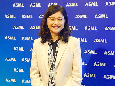
Netherlands-based semiconductor equipment supplier ASML Holding NV yesterday said that it is planning to hire an additional 1,000 people in Taiwan this year in response to growing demand from clients. ASML had previously planned to recruit 600 people this year, but that the plan has been adjusted upward, ASML vice president and ASML Taiwan general manager Grace Wang (汪佳慧) told reporters. ASML has a workforce of more than 4,500 in Taiwan, accounting for about 10 percent of its global total, Wang said. This year’s recruitment campaign would focus on adding people in the customer support, manufacturing and supply chain domains to assist ASML
UNDER MICROSCOPE: Taiwan detained three people who allegedly conspired to buy servers in Taiwan and export them using fraudulent documentation, prosecutors said Nvidia Corp chief executive officer Jensen Huang (黃仁勳) on Saturday urged Super Micro Computer Inc to tighten up on compliance after Taiwan detained three people this week for allegedly making fraudulent declarations about artificial intelligence (AI) servers made by its US partner. The development marked the nation’s first crackdown on semiconductor smuggling, which grew after the US slapped restrictions on exports of high-end chips such as Nvidia AI accelerators to China. Nvidia is “rigorous” in explaining regulations to all of its partners, Huang told reporters after arriving in Taipei. “Ultimately Super Micro has to run their own company,” he said in response to

Nvidia Corp yesterday announced that CEO Jensen Huang (黃仁勳) would attend an employee meeting in Taipei tomorrow to celebrate the launch of the company’s Taiwan headquarters project. Huang would attend a gathering at the site of Nvidia’s planned headquarters in Beitou Shilin Technology Park (北投士林科技園區), the company said in a statement. After arriving in Taiwan on Saturday last week, Huang told reporters that he plans to meet with Quanta Computer Inc (廣達) chairman Barry Lam (林百里) and Taiwan Semiconductor Manufacturing Co (TSMC, 台積電) chairman C.C. Wei (魏哲家), and would attend the groundbreaking ceremony for Nvidia’s Taiwan headquarters tomorrow. Nvidia has not yet applied