The US is tightening restrictions on China’s access to chipmaking gear, two major equipment suppliers have said, underscoring Washington’s accelerating efforts to curb Beijing’s economic ambitions.
Washington had banned the sale of most gear that can fabricate chips of 10 nanometers or better to Chinese firm Semiconductor Manufacturing International Corp (SMIC, 中芯國際) without a license.
Now it has expanded that barrier to equipment that can make anything more advanced than 14 nanometers, Lam Research Corp chief executive officer Tim Archer told analysts.
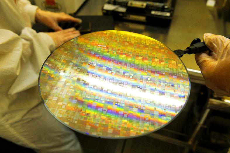
Photo: Bloomberg
The moratorium likely extends beyond SMIC and includes other fabrication plants run by contract chipmakers operating in China, including those by Taiwan Semiconductor Manufacturing Co (TSMC, 台積電).
“We were recently notified that there was to be a broadening of the restrictions of technology shipments to China for fabs that are operating below 14 nanometers,” Archer said during a conference call on Wednesday. “That’s the change, I think, people have been thinking might be coming and we’re prepared to fully comply. We’re working with the US government.”
In chip manufacturing, production identified by lower numbers of nanometers is more advanced. That means raising the restriction level to 14 nanometers would cover a broader range of semiconductor equipment.
The US Department of Commerce said in a statement that the administration of US President Joe Biden is tightening policies aimed at the People’s Republic of China (PRC), without specifying the precise chip geometry.
“The Biden administration is focused on impairing PRC efforts to manufacture advanced semiconductors to address significant national security risks to the United States,” the agency said.
All US equipment makers have in the past few weeks received letters from the commerce department telling them not to supply gear to Chinese firms for manufacturing at 14 nanometers or below, people familiar with the matter said.
The letters are at least partly an effort by the Biden administration to look tough on China, but the department had already declined many licenses at 14 nanometers so the change would have little financial effects, they said.
The new requirements are targeted at foundries — facilities making logic chips for others — and exclude memory chips “to the best of our understanding,” Archer said.
Lam Research executives said they had incorporated the expected effects of the US requirements into their outlook for the third quarter of this year, without elaborating.
KLA Corp CEO Rick Wallace on Thursday confirmed that his company had been notified by the US government of the change in export licensing requirements on China-bound gear for chips more advanced than 14 nanometers.
Wallace said there was no material impact on KLA’s business.
The comments from the two California-based companies mark the first detailed confirmation that the Biden administration is ramping up attempts to contain China. The US is pushing partner countries such as the Netherlands and Japan to ban ASML Holding NV and Nikon Corp from selling mainstream technology essential in making a large chunk of the world’s chips to China.
The new rules cover a wider swath of semiconductors across a plethora of industries and possibly affect far more companies than standing restrictions targeted at SMIC. While the new curbs specifically cover equipment capable of making chips more advanced than 14 nanometers, mature chips could still be affected, as about 90 percent of gear is compatible from one generation to the next. Semiconductor manufacturers can reuse equipment as they migrate to more sophisticated nodes, meaning a ban on one generation could have longer-term ripple effects.
SMIC’s most sophisticated technology is 14 nanometers, while the best TSMC uses in China is 16 nanometers. Those are three generations behind the most cutting-edge technology TSMC uses in Taiwan.
The new rules are likely to affect SMIC, TSMC and any others with the ambition to build capacity for relatively advanced chips in China, as well as gear makers such as Applied Materials Inc, ASML and Tokyo Electron Ltd, which sell to the world’s largest chip market.

Taiwanese firms have increased investment in the Philippines in recent years as Manila’s ties with Washington deepen and global supply chains continue to shift away from China, an expert at the Chung-Hua Institution for Economic Research (CIER, 中華經濟研究院) said yesterday. The Philippines had not been among Taiwanese investors’ top choices in Southeast Asia, CIER Taiwan ASEAN Studies Center director Kristy Hsu (徐遵慈) said at a seminar in Taipei. However, Taiwan’s investment in the country has grown significantly since the COVID-19 pandemic, reaching US $257 million last year, a high in recent years, she said. Although Taiwan’s total investment in the Philippines still lags
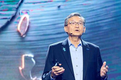
Intel Corp regards Taiwan Semiconductor Manufacturing Co (TSMC, 台積電) as a longstanding partner, as the US chipmaker would continue outsourcing production of advanced chips to TSMC, Intel chief executive officer Lip-Bu Tan (陳立武) said yesterday. “I don’t look at people as competitors. I look at the collaboration... Nvidia is also, you know, a good friend,” Tan told a news conference following his keynote speech at the Computex trade show in Taipei. “It’s a very trusted partnership for us... We are a big, top customer for them, and we’re going to continue doing that,” he said, referring to TSMC, the world’s largest foundry
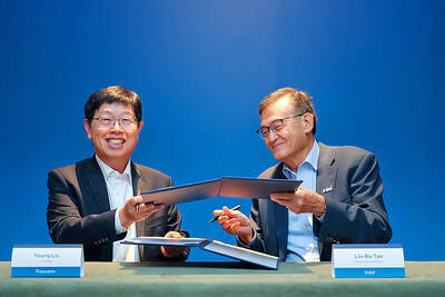
Hon Hai Precision Industry Co (鴻海精密) yesterday said it would work with US chipmaker Intel Corp to jointly develop and deploy next-generation artificial intelligence (AI) infrastructure and intelligent computing platforms in a move to capture booming demand for AI computing systems. Hon Hai, also known as Foxconn Technology Group (富士康), said in a statement that the partnership would combine its global manufacturing scale, system integration expertise and AI data center deployment capabilities with Intel’s strengths in processor architecture, silicon technologies and software ecosystem. The companies said they plan to work on equipment used in AI data centers, including server racks powered by

Artificial intelligence (AI) agents would supplant smartphones as the center of people’s digital lives, fundamentally reshaping personal devices and driving a major computing upgrade cycle, Qualcomm Inc CEO Cristiano Amon said yesterday. In his keynote speech for this year’s Computex trade show in Taipei, Amon said that the rise of "agentic AI" — AI systems capable of reasoning, planning and carrying out tasks autonomously — would transform how people interact with technology across phones, PCs, vehicles and wearable devices. Describing the technology as the next major evolution in computing, Amon said that "2026 is the year of agents.” For decades, smartphones have sat