Intel Corp yesterday said it has placed its first order with ASML Holding NV to purchase the semiconductor industry’s first TWINSCAN EXE: 5200 system, as the US chip giant aims to compete with Taiwan Semiconductor Manufacturing Co (TSMC, 台積電) in advancing to 2-nanometer process technology.
The Dutch semiconductor equipment maker’s TWINSCAN EXE:5200 system is an extreme ultraviolet (EUV) high-volume production system with a high numerical aperture (NA) that can produce 220 wafers per hour, more than the 150 wafers that its previous generation TWINSCAN EXE:5000 system can handle.
ASML aims to launch the new system in 2024.
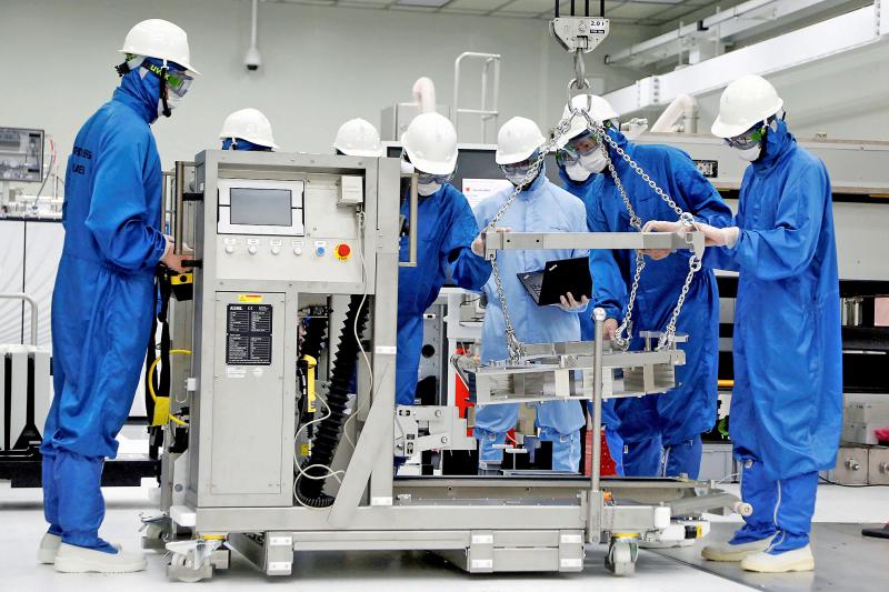
Photo: Reuters
ASML president and chief technology officer Martin van den Brink said in a statement that the new system “delivers continued lithographic improvements at reduced complexity, cost, cycle time and energy that the chip industry needs to drive affordable scaling well into the next decade.”
Announcing the deal in a statement, Intel executive vice president and general manager of technology development Ann Kelleher said: “Working closely with ASML, we will harness high-NA EUV’s high-resolution patterning as one of the ways we continue Moore’s Law and maintain our strong history of progression down to the smallest of geometries.”
Intel was the first to purchase the TWINSCAN EXE:5000 system in 2018.
The company said that the new purchase reflects its continued collaboration with ASML and marks the beginning of its production with the new technology in 2025.
TSMC is also likely to buy the TWINSCAN EXE:5200 system and is expected to be the first in the industry to introduce 2-nanometer production, a supply chain source told the Taipei Times yesterday.
“Placing the first order does not mean Intel will be the first to massively produce chips with the tool,” the source said, adding that Intel still has a long way to go before catching up with TSMC in commercializing 2-nanometer technology.
TSMC’s 2-nanometer chips would enter the market in 2025, the firm said, adding that the chips would be the highest-performing chips available.
Separately, ASML yesterday said that it did not expect a factory fire in Germany to disrupt output.
The fire at its Berlin facility early this month was extinguished within two hours, and the company still expects to ship about 55 EUV systems this year, it said.
“We were able to put the fire out in a couple of hours, but still there was significant damage,” ASML chief executive officer Peter Wennink said in a statement. “Because of the hard work and the creativity, we currently believe that we can manage the situation and that we will not see a significant impact on our EUV output in the year 2022.”
Wennink said demand is 40 to 50 percent above the ASML’s maximum capacity, and it would take “two to three years to get a nice balance between supply and demand.”
The firm’s shipments would increase next year, he added.
Additional reporting by Bloomberg

Taichung reported the steepest fall in completed home prices among the six special municipalities in the first quarter of this year, data compiled by Taiwan Realty Co (台灣房屋) showed yesterday. From January through last month, the average transaction price for completed homes in Taichung fell 8 percent from a year earlier to NT$299,000 (US$9,483) per ping (3.3m²), said Taiwan Realty, which compiled the data based on the government’s price registration platform. The decline could be attributed to many home buyers choosing relatively affordable used homes to live in themselves, instead of newly built homes in the city’s prime property market, Taiwan Realty

The government yesterday approved applications by Alphabet Inc’s Google to invest NT$27.08 billion (US$859.98 million) in Taiwan, the Ministry of Economic Affairs said in a statement. The Department of Investment Review approved two investments proposed by Google, with much of the funds to be used for data processing and electronic information supply services, as well as inventory procurement businesses in the semiconductor field, the ministry said. It marks the second consecutive year that Google has applied to increase its investment in Taiwan. Google plans to infuse NT$25.34 billion into Charter Investments Ltd (特許投資顧問) through its Singapore-based subsidiary Fructan Holdings Singapore Pte Ltd, and

Micron Technology Inc is a driving force pushing the US Congress to pass legislation that would put new export restrictions on equipment its Chinese competitors use to make their chips, according to people familiar with the matter. A US House of Representatives panel yesterday was to vote on the “MATCH Act,” a bill designed to close gaps in restrictions on chipmaking equipment. It would also pressure foreign companies that sell equipment to Chinese chipmaking facilities to align with export curbs on US companies like Lam Research Corp and Applied Materials Inc. The bill targets facilities operated by China’s ChangXin Memory Technologies Inc

Singapore-based ride-hailing and delivery giant Grab Holdings’ planned acquisition of Foodpanda’s Taiwan operations has yet to enter the formal review stage, as regulators await supplementary documents, the Fair Trade Commission (FTC) said yesterday. Acting FTC Chairman Chen Chih-min (陳志民) told the legislature’s Economics Committee that although Grab submitted its application on March 27, the case has not been officially accepted because required materials remain incomplete. Once the filing is finalized, the FTC would launch a formal probe into the deal, focusing on issues such as cross-shareholding and potential restrictions on market competition, Chen told lawmakers. Grab last month announced that it would acquire