Intel Corp has talked with Taiwan Semiconductor Manufacturing Co (TSMC, 台積電) and Samsung Electronics Co about the Asian companies making some of its best chips, but the Silicon Valley pioneer is still holding out hope for last-minute improvements in its own production capabilities.
After successive delays in its chip fabrication processes, Santa Clara, California-based Intel has yet to make a decision less than two weeks ahead of a scheduled announcement of its plans, people familiar with the deliberations said.
Any components that Intel might source from Taiwan would not come to market until 2023 at the earliest and would be based on established manufacturing processes already in use by other TSMC customers, said the people, asking not to be identified because the plans are private.
Photo: Ashley Pon, Bloomberg
Talks with Samsung, whose foundry capabilities trail TSMC’s, are at a more preliminary stage, the people said.
TSMC and Samsung representatives declined to comment, while an Intel spokesperson referred to previous comments by CEO Bob Swan, who has promised investors he would set out his plans for outsourcing and putting Intel’s production technology back on track when the company reports earnings on Thursday next week.
TSMC, the largest maker of semiconductors for other companies, is preparing to offer Intel chips manufactured using a 4-nanometer process, with initial testing using an older 5-nanometer process, the people said.
The company has said it would make test production of 4-nanometer chips available in the fourth quarter of this year and volume shipments the following year.
TSMC expects to have a new facility in Hsinchu County’s Baoshan Township (寶山) operational by the end of this year, which can be converted to production for Intel if required, one of the people said.
TSMC executives previously said the Baoshan unit would house a research center with 8,000 engineers.
Intel’s strategic shifts are happening at a time of booming demand, as well as technological change in the chip industry.
The traditional method of improving performance by shrinking and cramming more transistors into each package is being supplanted by more sophisticated techniques that include stacking processor and memory components into single chips and the introduction of more tailored designs for tasks like artificial intelligence.
Separately, United Microelectronics Corp (UMC, 聯電) on Saturday had power-supply disruptions at two plants in Hsinchu that temporarily affected production, UMC chief financial officer Liu Chi-tung (劉啟東) said.
“The company will discuss with customers, and try its best to make up for lost production,” Liu said by telephone. “No major financial impact is expected.”
The overall impact of the incident was “quite minor,” Liu said.
Power was being gradually restored, he said.
Taiwan Semiconductor Manufacturing Co (TSMC, 台積電) has approved a capital budget of US$31.28 billion for production expansion to meet long-term development needs during the artificial intelligence (AI) boom. The company’s board meeting yesterday approved the capital appropriation plan for purposes such as the installation of advanced technology capacity and fab construction, the world’s largest contract chipmaker said in a statement. At an earnings conference last month, TSMC forecast that its capital expenditure for this year would be at the higher end of the US$52 billion to US$56 billion range it forecast in January in response to robust demand for 5G, AI and
PORTFOLIO REBALANCING: The adjustments in three global equity indices reflect rising investor appetite for semiconductor and artificial intelligence-related stocks Taiwan’s weighting in major global equity indices compiled by MSCI Inc is to rise modestly following the latest quarterly review, underscoring the market’s expanding role in emerging-market portfolios, as global investors continue to favor the nation’s technology sector. Taiwan’s weighting in the MSCI Emerging Markets Index is to increase by 0.30 percentage points to 23.76 percent, after the changes take effect at the close of the May 29 session. Its weighting in the MSCI All-Country Asia ex-Japan Index is to rise 0.37 percentage points to 27.16 percent, while that in the MSCI All Country World Index is to edge up slightly to
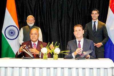
NEW MARKET: The partnership opens up India to the Dutch company, which already has a strong hold in the semiconductor market of South Korea, Taiwan and China ASML Holding NV entered into a partnership agreement with Tata Electronics Pvt Ltd aimed at ramping up India’s goal to develop domestic chip-manufacturing capabilities. The Dutch company’s technology would help power Tata Electronics’ planned 300 millimeter (mm) semiconductor foundry in Gujarat, according to a joint statement from the two companies on Saturday. The signing of a memorandum of understanding coincides with a visit by Indian Prime Minister Narendra Modi to the Netherlands, which is looking to deepen bilateral relations with New Delhi. ASML, whose top customers include Taiwan Semiconductor Manufacturing Co (台積電) and Samsung Electronics Co, makes lithography machines that can print
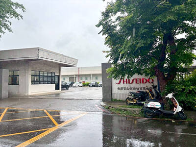
The Hsinchu County Government’s Labor Affairs Department yesterday said that it has received a plan from cosmetics brand Taiwan Shiseido Co (台灣資生堂) detailing mass layoffs at its plant in Hukou Township (湖口). While the labor authorities did not disclose the number of employees to be laid off, Japanese news media earlier in the day reported that the closure of the company’s factory in Hukou would result in 170 employees losing their jobs. Shiseido followed the law by reporting its layoff plan, the department said, adding that authorities would closely monitor negotiations between the management and affected employees and step in if any