Taiwan Semiconductor Manufacturing Co’s (TSMC, 台積電) plan to build an advanced wafer foundry in Arizona would not undercut its technological edge in Taiwan, economists said.
“When the planned Arizona plant using the 5 nanometer process starts production in 2024, TSMC will have advanced to the 2 nanometer process [in Taiwan],” Taiwan Institute of Economic Research (TIER, 台灣經濟研究院) research fellow Arisa Liu (劉佩真) said.
“Even if the US has the plant run by TSMC, Taiwan is expected to remain competitive as the Taiwanese semiconductor sector will own advanced technologies,” Liu said.
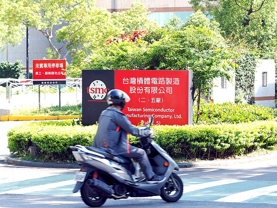
Photo: David Chang, EPA-EFE
On Friday, TSMC announced plans to invest US$12 billion to build the 5 nanometer fab, saying that construction is scheduled to start next year.
The 5 nanometer process is currently the world’s most advanced mass production process, but the company is developing a more sophisticated 3 nanometer process that could start mass production in 2022.
Liu said that TSMC’s 5 nanometer plant in Taiwan is expected to produce 80,000 wafers a month by the end of this year, four times the capacity of the planned US facility, and that is likely to grow next year.
At the same time, the investment in Arizona falls short of TSMC’s annual capital expenditure of between US$15 billion and US$16 billion, Liu added.
“So whether you look at [capital expenditure] or output,” TSMC and, by extension, Taiwan’s semiconductor industry, should maintain its lead, Liu said.
Stephen Su (蘇孟宗), head of the government-sponsored Industrial Technology Research Institute’s (工研院) Industrial Economics and Knowledge Center, said that TSMC chose Arizona as it is home to several semiconductor plants, including Intel Corp and NXP Semiconductors NV.
This would provide TSMC an existing supply chain to work with, Su said.
The state also has the advantages of dry weather and few natural disasters, such as earthquakes, Su said, adding that the higher labor costs in the US are not expected to be a problem because foundries are highly automated through cloud-based technologies.
Liu said that the proposed investment was likely a necessary move, because US-based businesses account for about 60 percent of its sales, and rising trade tensions between the US and China could force producers to move some production to the US.
Separately, Chinese state-backed funds pumped US$2.25 billion into a Semiconductor Manufacturing International Corp (SMIC, 中芯國際) wafer plant to support advanced chip manufacturing, as Washington tightens technology restrictions on China.
The SMIC plant’s registered capital jumped from US$3.5 billion to US$6.5 billion after the investment, the company said in an announcement on Friday.
The chipmaker’s stake in the Shanghai facility would fall from 50.1 percent to 38.5 percent, it said.
The plant has capacity to produce 6,000 14 nanometer wafers a month and plans to increase that to 35,000.
The investment came as Washington moved to prevent sales to Huawei Technologies Co (華為) from chipmakers using US technology.
The US Department of Commerce on Friday said it would require licenses before allowing US technology to be used by the Chinese company or its 114 subsidiaries, including its chip-design unit HiSilicon Technologies Co (海思半導體).
SMIC is planning a Shanghai share sale that could raise more than US$3 billion, based on its closing value of more than US$13 billion on Friday.
China is betting the local chipmaker could reduce the country’s reliance on US technology.

Taiwanese firms have increased investment in the Philippines in recent years as Manila’s ties with Washington deepen and global supply chains continue to shift away from China, an expert at the Chung-Hua Institution for Economic Research (CIER, 中華經濟研究院) said yesterday. The Philippines had not been among Taiwanese investors’ top choices in Southeast Asia, CIER Taiwan ASEAN Studies Center director Kristy Hsu (徐遵慈) said at a seminar in Taipei. However, Taiwan’s investment in the country has grown significantly since the COVID-19 pandemic, reaching US $257 million last year, a high in recent years, she said. Although Taiwan’s total investment in the Philippines still lags
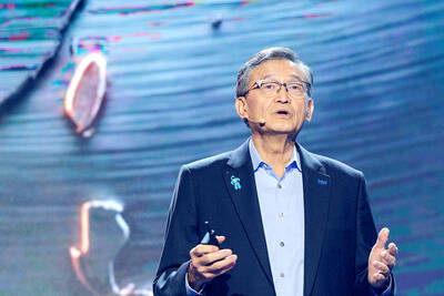
Intel Corp regards Taiwan Semiconductor Manufacturing Co (TSMC, 台積電) as a longstanding partner, as the US chipmaker would continue outsourcing production of advanced chips to TSMC, Intel chief executive officer Lip-Bu Tan (陳立武) said yesterday. “I don’t look at people as competitors. I look at the collaboration... Nvidia is also, you know, a good friend,” Tan told a news conference following his keynote speech at the Computex trade show in Taipei. “It’s a very trusted partnership for us... We are a big, top customer for them, and we’re going to continue doing that,” he said, referring to TSMC, the world’s largest foundry
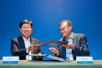
Hon Hai Precision Industry Co (鴻海精密) yesterday said it would work with US chipmaker Intel Corp to jointly develop and deploy next-generation artificial intelligence (AI) infrastructure and intelligent computing platforms in a move to capture booming demand for AI computing systems. Hon Hai, also known as Foxconn Technology Group (富士康), said in a statement that the partnership would combine its global manufacturing scale, system integration expertise and AI data center deployment capabilities with Intel’s strengths in processor architecture, silicon technologies and software ecosystem. The companies said they plan to work on equipment used in AI data centers, including server racks powered by
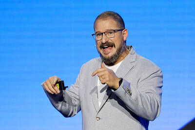
Artificial intelligence (AI) agents would supplant smartphones as the center of people’s digital lives, fundamentally reshaping personal devices and driving a major computing upgrade cycle, Qualcomm Inc CEO Cristiano Amon said yesterday. In his keynote speech for this year’s Computex trade show in Taipei, Amon said that the rise of "agentic AI" — AI systems capable of reasoning, planning and carrying out tasks autonomously — would transform how people interact with technology across phones, PCs, vehicles and wearable devices. Describing the technology as the next major evolution in computing, Amon said that "2026 is the year of agents.” For decades, smartphones have sat