IBM Corp said on Thursday that it had made working versions of ultradense computer chips, with roughly four times the capacity of the most powerful chips on the market.
The announcement, made on behalf of an international consortium led by computer giant IBM, is part of an effort to manufacture advanced computer chips in New York’s Hudson Valley, where IBM is investing US$3 billion in a private-public partnership with New York State, GlobalFoundries Inc, Samsung Electronics Co and equipment vendors.
The development lifts a bit of the cloud that has fallen over the semiconductor industry, which has struggled to maintain its legendary pace of doubling transistor density every two years.
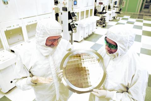
Photo: AP
Intel, which for decades has been the industry leader, has faced technical challenges in recent years. Moreover, technologists have begun to question whether the longstanding pace of chip improvement, known as Moore’s Law, would continue past the current 14 nanometer (nm) generation of chips.
Each generation of chip technology is defined by the minimum size of fundamental components that switch current at nanosecond intervals. Today the industry is making the commercial transition from what the industry generally describes as 14nm manufacturing to 10nm manufacturing.
Each generation brings roughly a 50 percent reduction in the area required by a given amount of circuitry. IBM’s new chips, though still in a research phase, suggest semiconductor technology will continue to shrink at least through 2018.
The company said that it has working samples of chips with 7nm transistors. It made the research advance by using silicon-germanium instead of pure silicon in key regions of the molecule-sized switches.
The new material makes possible faster transistor switching and lower power requirements. The tiny size of these transistors suggests further advances will require new materials and new manufacturing techniques.
As points of comparison to the size of the 7nm transistors, a strand of DNA is about 2.5nm in diameter and a red blood cell is roughly 7,500nm in diameter.
IBM said that would make it possible to build microprocessors with more than 20 billion transistors.
“I’m not surprised, because this is exactly what the road map predicted, but this is fantastic,” said Subhashish Mitra, director of the Robust Systems Group at Stanford University’s Electrical Engineering Department.
Even though IBM has shed much of its computer and semiconductor manufacturing capacity, the announcement indicates the company remains interested in supporting the US’ high-tech manufacturing base.
“This puts IBM in the position of being a gentleman gambler as opposed to being a horse owner,” said Richard Doherty, president of Envisioneering, a Seaford, New York-based consulting firm, referring to the fact that IBM’s chip manufacturing facility was acquired by GlobalFoundries.
“They still want to be in the race,” he added.
IBM licenses the technology it is developing to a number of manufacturers and GlobalFoundries, owned by the Emirate of Abu Dhabi, to make chips for companies including Broadcom Corp, Qualcomm Inc and Advanced Micro Devices Inc.
The semiconductor industry must now decide if IBM’s bet on silicon-germanium is the best way forward. It must also grapple with the shift to using extreme ultraviolet light to etch patterns on chips at a resolution that approaches the diameter of individual atoms.
In the past, Intel said it could see its way toward 7nm manufacturing. However, it has not said when that generation of chipmaking might arrive.
IBM also declined to speculate on when it might begin commercial manufacturing of this technology generation. This year, Taiwan Semiconductor Manufacturing Co (台積電) said it planned to begin pilot product of 7nm chips in 2017. However, unlike IBM, it has not demonstrated working chips to meet that goal.

Among the rows of vibrators, rubber torsos and leather harnesses at a Chinese sex toys exhibition in Shanghai this weekend, the beginnings of an artificial intelligence (AI)-driven shift in the industry quietly pulsed. China manufactures about 70 percent of the world’s sex toys, most of it the “hardware” on display at the fair — whether that be technicolor tentacled dildos or hyper-realistic personalized silicone dolls. Yet smart toys have been rising in popularity for some time. Many major European and US brands already offer tech-enhanced products that can enable long-distance love, monitor well-being and even bring people one step closer to

Malaysia’s leader yesterday announced plans to build a massive semiconductor design park, aiming to boost the Southeast Asian nation’s role in the global chip industry. A prominent player in the semiconductor industry for decades, Malaysia accounts for an estimated 13 percent of global back-end manufacturing, according to German tech giant Bosch. Now it wants to go beyond production and emerge as a chip design powerhouse too, Malaysian Prime Minister Anwar Ibrahim said. “I am pleased to announce the largest IC (integrated circuit) Design Park in Southeast Asia, that will house world-class anchor tenants and collaborate with global companies such as Arm [Holdings PLC],”

TRANSFORMATION: Taiwan is now home to the largest Google hardware research and development center outside of the US, thanks to the nation’s economic policies President Tsai Ing-wen (蔡英文) yesterday attended an event marking the opening of Google’s second hardware research and development (R&D) office in Taiwan, which was held at New Taipei City’s Banciao District (板橋). This signals Taiwan’s transformation into the world’s largest Google hardware research and development center outside of the US, validating the nation’s economic policy in the past eight years, she said. The “five plus two” innovative industries policy, “six core strategic industries” initiative and infrastructure projects have grown the national industry and established resilient supply chains that withstood the COVID-19 pandemic, Tsai said. Taiwan has improved investment conditions of the domestic economy

MAJOR BENEFICIARY: The company benefits from TSMC’s advanced packaging scarcity, given robust demand for Nvidia AI chips, analysts said ASE Technology Holding Co (ASE, 日月光投控), the world’s biggest chip packaging and testing service provider, yesterday said it is raising its equipment capital expenditure budget by 10 percent this year to expand leading-edge and advanced packing and testing capacity amid strong artificial intelligence (AI) and high-performance computing chip demand. This is on top of the 40 to 50 percent annual increase in its capital spending budget to more than the US$1.7 billion to announced in February. About half of the equipment capital expenditure would be spent on leading-edge and advanced packaging and testing technology, the company said. ASE is considered by analysts