A South Korean court said studies conducted to evaluate safety at Samsung Electronics Co’s chip factories failed to fully examine workplace health hazards, undermining the electronics giant’s efforts to distance itself from claims that its manufacturing plants caused cancers.
The finding by the Seoul Administrative Court was part of a ruling in the case of a Samsung worker who died of leukemia in 2009 at age 29.
A panel of three judges said that a “considerable causal relationship” existed between Kim Kyung-mi’s leukemia and her five years of work at a Samsung memorychip factory, dipping wafers in chemicals.
The judges said that Kim must have been exposed to more toxic chemicals than safety studies said existed at Samsung’s factories.
Samsung, one of the best known South Korean companies and a powerful force in the country’s economy, has cited studies that found no dangerous level of benzene, formaldehyde or other carcinogens to ease public concerns about workplace hazards.
However, the studies did not evaluate exposure to chemicals during maintenance work, blackouts, gas leaks or other incidents when the level of toxic gas goes up sharply, the judges said.
The court ordered the Korea Workers’ Compensations & Welfare Service, a government agency, to pay compensation to Kim’s family.
Claims for compensation for injuries and disease linked to the workplace are decided by the agency, which levies companies to fund its payouts. The agency had previously denied compensation to Kim’s family who appealed to the Seoul court.
The latest ruling is the second case in South Korea in which a court recognized a link between leukemia and working conditions at Samsung memorychip factories.
In 2011, a court said the deaths of two Samsung workers from leukemia were associated with their work at the company and ordered the government agency to pay compensation to their families. The agency appealed and the case is pending.
Kim worked at Samsung’s chip factory in Giheung from 1999 to 2004 on “Line 2,” which was one of the three oldest chip manufacturing lines at Samsung.
The two other workers who died of leukemia and won compensation from the government agency worked on these three lines, all of which were built during the 1980s.
Lee Jong-ran, an attorney who helps tech industry workers, said most leukemia deaths of Samsung workers were among employees who worked at the old lines. They were shut and renovated after 2006.
The judges said there was a “high probability” that benzene, formaldehyde or other leukemia-causing materials were contained in the chemicals Kim used, or created during the manufacturing process.
However, it said it was not possible to further determine Kim’s exposure to carcinogens partly because Samsung had not cooperated.
“Samsung Electronics, which did not preserve information of chemical materials used during Kim’s work and did not disclose some data citing trade secrets, is partly a cause,” according to the ruling.
Samsung was not a defendant in Kim’s case.
“While the court’s decision appears to have been based on probability, as a party that was not a part of the proceedings, we feel that it would be inappropriate for us to comment on the matter,” Samsung said in a statement.
“Regardless, Samsung’s top priority has always been ensuring the health and safety of every person we employ,” it said.
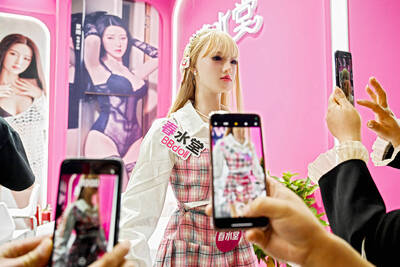
Among the rows of vibrators, rubber torsos and leather harnesses at a Chinese sex toys exhibition in Shanghai this weekend, the beginnings of an artificial intelligence (AI)-driven shift in the industry quietly pulsed. China manufactures about 70 percent of the world’s sex toys, most of it the “hardware” on display at the fair — whether that be technicolor tentacled dildos or hyper-realistic personalized silicone dolls. Yet smart toys have been rising in popularity for some time. Many major European and US brands already offer tech-enhanced products that can enable long-distance love, monitor well-being and even bring people one step closer to

TRANSFORMATION: Taiwan is now home to the largest Google hardware research and development center outside of the US, thanks to the nation’s economic policies President Tsai Ing-wen (蔡英文) yesterday attended an event marking the opening of Google’s second hardware research and development (R&D) office in Taiwan, which was held at New Taipei City’s Banciao District (板橋). This signals Taiwan’s transformation into the world’s largest Google hardware research and development center outside of the US, validating the nation’s economic policy in the past eight years, she said. The “five plus two” innovative industries policy, “six core strategic industries” initiative and infrastructure projects have grown the national industry and established resilient supply chains that withstood the COVID-19 pandemic, Tsai said. Taiwan has improved investment conditions of the domestic economy

Malaysia’s leader yesterday announced plans to build a massive semiconductor design park, aiming to boost the Southeast Asian nation’s role in the global chip industry. A prominent player in the semiconductor industry for decades, Malaysia accounts for an estimated 13 percent of global back-end manufacturing, according to German tech giant Bosch. Now it wants to go beyond production and emerge as a chip design powerhouse too, Malaysian Prime Minister Anwar Ibrahim said. “I am pleased to announce the largest IC (integrated circuit) Design Park in Southeast Asia, that will house world-class anchor tenants and collaborate with global companies such as Arm [Holdings PLC],”

MAJOR BENEFICIARY: The company benefits from TSMC’s advanced packaging scarcity, given robust demand for Nvidia AI chips, analysts said ASE Technology Holding Co (ASE, 日月光投控), the world’s biggest chip packaging and testing service provider, yesterday said it is raising its equipment capital expenditure budget by 10 percent this year to expand leading-edge and advanced packing and testing capacity amid strong artificial intelligence (AI) and high-performance computing chip demand. This is on top of the 40 to 50 percent annual increase in its capital spending budget to more than the US$1.7 billion to announced in February. About half of the equipment capital expenditure would be spent on leading-edge and advanced packaging and testing technology, the company said. ASE is considered by analysts