

The next phase of artificial intelligence (AI) growth would be driven by the large-scale deployment of integrated computing systems as the industry enters the “true industrialization of AI,” Taiwan Semiconductor Manufacturing Co (TSMC, 台積電) AI and high-performance computing business development director April Li (李湘) said yesterday.
AI agents are moving into enterprise workflows, while investment in specialized data centers and physical AI is accelerating, Li said in a keynote speech at the Semicon Taiwan IC forum in Taipei.
“In this new era, market leaders will not be the ones who simply make better models, but those who build the most integrated systems,” Li said.
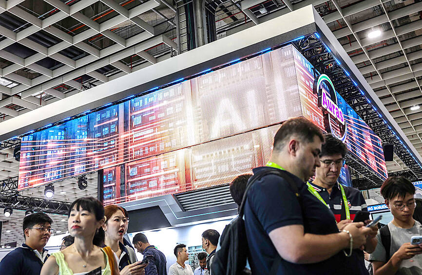
Photo: I-Hwa Cheng, AFP
Rather than relying on advances in individual chips or models alone, future AI infrastructure would increasingly need to integrate computing, memory, interconnects, storage and power management across chips, server racks and entire data centers, she said.
The shift is being driven partly by soaring demand for AI inference — the process of using trained models to respond to requests and perform tasks, Li said.
Global inference token volume has increased about 500-fold from its 2022 level, while more complex reasoning and agentic AI systems consume more tokens than conventional one-shot queries, she said.
“Inference is no longer a low-overhead task,” Li said, adding that it is becoming the dominant driver of system-level expansion as AI agents operate continuously in the background.
The growing workloads are putting pressure on four areas — logic scaling, interconnect efficiency, memory performance, and power delivery and cooling, she said.
Data movement alone can account for up to 60 percent of system activity in typical workloads, leaving accelerators operating at below 40 percent utilization, she added.
Meanwhile, AI packages might contain more than 1 trillion transistors by 2030, making multi-die architecture and heterogeneous integration essential, Li said.
To address those constraints, TSMC is developing technologies covering advanced logic, packaging and optical interconnects, she said.
She highlighted the chipmaker’s 3DFabric platform, which incorporates technologies such as system on integrated chips 3D stacking and chip-on-wafer-on-substrate advanced packaging, as well as its compact universal photonic engine platform for high-speed optical data transmission.
TSMC is also working to improve high-bandwidth memory performance by using advanced logic technology in high-bandwidth memory base dies, Li said.
In a question-and-answer session, Li said TSMC must develop an in-depth understanding of the supply chain “from silicon to the data center to the token” and work with ecosystem partners to validate its technologies as early as possible across that chain.
That reflects how TSMC’s role has expanded beyond manufacturing individual chips, she said.
“Gone are the days when we can just ship wafers across the fence,” Li said.

In China’s hilly Guizhou Province, a cluster of European-style buildings complete with clock tower and multi-arched bridge emits a low, permanent hum — a clue to its unexpected identity as tech giant Huawei’s largest data center. The town-like complex is unique in design, but not in its placement. Dozens of data centers have been constructed in the southwestern province in the past few years. They are part of a government strategy that has seen much of the digital infrastructure for breakneck artificial intelligence (AI) development across China’s eastern seaboard established in the country’s less populated, rural west. The build-out is ongoing. China
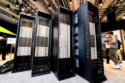
AM Intelligence, an Indian artificial intelligence (AI) infrastructure company, has ordered 9,000 Nvidia Corp Vera Rubin systems, seeking to become one of the first adopters of the advanced computing platform in Asia. Servers equipped with the rack-scale systems are slated to come online next year in southern India, the Hyderabad-based company said in a statement yesterday. Customers include major cloud service providers, AI labs and organizations aiming to develop homegrown Indian AI models, it said. Supplies of high-end Nvidia compute clusters remain tight. Demand from data centers and companies such as Microsoft Corp, Alphabet Inc’s Google and Amazon.com Inc to train AI models
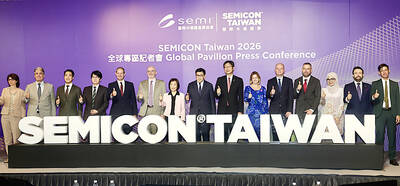
EXPANDING: Firms are accelerating commercialization of the technologies as the industry moves beyond chip-level speeds to upgrading rack-to-rack links, SEMI said Silicon photonics and copackaged optics (CPO), technologies seen as critical to meeting the surging bandwidth demands of artificial intelligence (AI) infrastructure, would be among the main themes at the Semicon Taiwan trade show, which opens on Wednesday, event organizer SEMI said yesterday. The forum runs until Friday at the Taipei Nangang Exhibition Center, with technical forums beginning today. The event is expected to set a record in terms of the number of participants, SEMI said, projecting more than 1,300 exhibitors from 65 countries across 4,300 booths and more than 100,000 attendees. Optical interconnects underpinning AI infrastructure would be one of the highlights, with
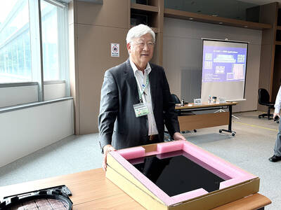
STRATEGIC GAMBLE: After developing FOPLP for six years, the chip packager has secured a 100 percent utilization rate for the new technology, its chairman said Chip packaging service provider Powertech Technology Inc (力成科技) yesterday said that its advanced fan-out panel-level packaging (FOPLP) production line has secured a 100 percent utilization rate through 2030 ahead of its scheduled volume production next year. Powertech made the remarks during the first public unveiling of its FOPLP production capabilities. The company expressed strong confidence in its long-term order pipeline, saying that robust market traction has mitigated any client acquisition concerns. “Our capacity has been fully booked by two major customers. Customers are not an issue through 2030,” Powertech chairman Tsai Du-kung (蔡篤恭) told reporters at the company’s plant in the Hsinchu


 RSS
RSS