Samsung Electronics Co unveiled a number of forthcoming advancements to its technology aimed at attracting makers of artificial intelligence (AI) chips.
Although, Samsung is the world’s No. 1 memorychip maker, it has been trying to catch up with rival Taiwan Semiconductor Manufacturing Co (TSMC, 台積電) in the foundry market, where companies manufacture customer-designed chips.
Samsung’s share in the foundry market slid to 11 percent in the first quarter of this year from 11.3 percent in the previous quarter, while TSMC’s share climbed to 61.7 percent from 61.2 percent during the same period, according to Taipei-based research house TrendForce Corp (集邦科技).
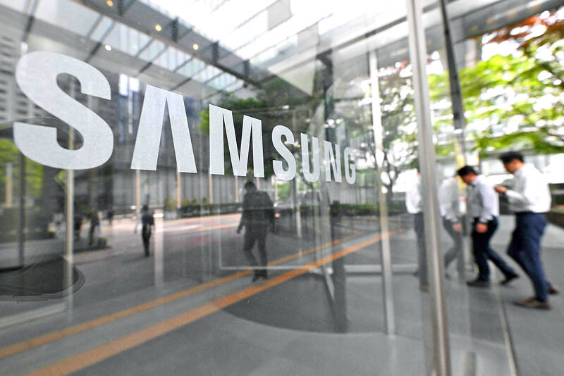
Photo: AFP
Samsung on Wednesday announced several new types of production technology and laid out its chipmaking road map and outlined its vision for the AI era at its annual foundry forum in San Jose, California.
The advanced process introduced by Samsung uses so-called backside power delivery network technology, which places power rails on the backside of a silicon wafer. Such technology enhances power, performance and area, while significantly reducing the drop in voltage, compared with its first-generation 2-nanometer process, the company said.
The South Korean chipmaker also said that its ability to offer logic, memory and advanced packaging would help it make rapid progress in winning outsourced semiconductor manufacturing orders for AI-related chips.
The company predicted that its AI-related customer list would expand five-fold and revenue would increase by nine times over current levels by 2028.
Samsung executives declined to comment on the status of the company’s attempts to supply the latest advanced memory chips to Nvidia Corp, which produces AI accelerators that are a must-have for all large technology companies.
They also did not respond to reports that it has not yet been able to achieve qualification of such chips at the US company.
The company touted its gate-all-around (GAA) technology, which is key for AI products.
Samsung said it plans to mass produce its second-generation 3-nanometer process in the second half of this year and deliver GAA on its upcoming 2-nanometer process.
In 2022, the company became the first in the industry to begin GAA-based 3-nanometer mass production.
The chipmaker affirmed that its preparations for 1.4-nanometer are progressing smoothly, with performance and yield targets on track for mass production in 2027.

Shares of contract chipmaker Taiwan Semiconductor Manufacturing Co (TSMC, 台積電) came under pressure yesterday after a report that Apple Inc is looking to shift some orders from the Taiwanese company to Intel Corp. TSMC shares fell NT$55, or 2.4 percent, to close at NT$2,235 on the local main board, Taiwan Stock Exchange data showed. Despite the losses, TSMC is expected to continue to benefit from sound fundamentals, as it maintains a lead over its peers in high-end process development, analysts said. “The selling was a knee-jerk reaction to an Intel-Apple report over the weekend,” Mega International Investment Services Corp (兆豐國際投顧) analyst Alex Huang
Taiwan Semiconductor Manufacturing Co (TSMC, 台積電) is expected to remain Apple Inc’s primary chip manufacturing partner despite reports that Apple could shift some orders to Intel Corp, industry experts said yesterday. The comments came after The Wall Street Journal reported on Friday that Apple and Intel had reached a preliminary agreement following more than a year of negotiations for Intel to manufacture some chips for Apple devices. Taiwan Institute of Economic Research (台灣經濟研究院) economist Arisa Liu (劉佩真) said TSMC’s advanced packaging technologies, including integrated fan-out and chip-on-wafer-on-substrate, remain critical to the performance of Apple’s A-series and M-series chips. She said Intel and Samsung
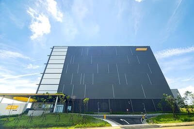
POWER BUILDUP: Powered by Nvidia’s B200 Blackwell chips, the data center would support MediaTek’s computing power demand and business growth, the company said Smartphone chip designer MediaTek Inc (聯發科) yesterday launched a new artificial intelligence (AI) data center with a maximum capacity of 45 megawatts to meet its rising demand for computing power required to develop new advanced chips for AI applications. The company has completed the first-phase computing power buildup at the data center in Miaoli County’s Tongluo Township (銅鑼), providing 15 megawatts of capacity to support its research and development (R&D) capabilities, despite an industrywide shortage of key components, MediaTek said. Supply constraints have plagued a wide range of key components, including memory chips, solid-state drives, power supply units and central
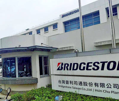
TRANSITION: With the closure, the company would reorganize its Taiwanese unit to a sales and service-focused model, Bridgestone said Bridgestone Corp yesterday announced it would cease manufacturing operations at its tire plant in Hsinchu County’s Hukou Township (湖口), affecting more than 500 workers. Bridgestone Taiwan Co (台灣普利司通) said in a statement that the decision was based on the Tokyo-based tire maker’s adjustments to its global operational strategy and long-term market development considerations. The Taiwanese unit would be reorganized as part of the closure, effective yesterday, and all related production activities would be concluded, the statement said. Under the plan, Bridgestone would continue to deepen its presence in the Taiwanese market, while transitioning to a sales and service-focused business model, it added. The Hsinchu