India’s government has approved US$15.2 billion worth of investments in semiconductor fabrication plants, including a Tata Group proposal to build the country’s first major chipmaking facility.
Indian Prime Minister Narendra Modi’s Cabinet approved Tata’s plan to build a US$11 billion site that can fabricate about 50,000 wafers per month, Indian Minister of Railways, Communications and Electronics and Information Technology Ashwini Vaishnaw told reporters in New Delhi yesterday.
The Indian government also cleared Tata’s separate proposal for a US$3 billion-plus chip assembly plant, and a packaging venture between Japan’s Renesas Electronics Corp and the Murugappa Group’s CG Power and Industrial Solutions Ltd.
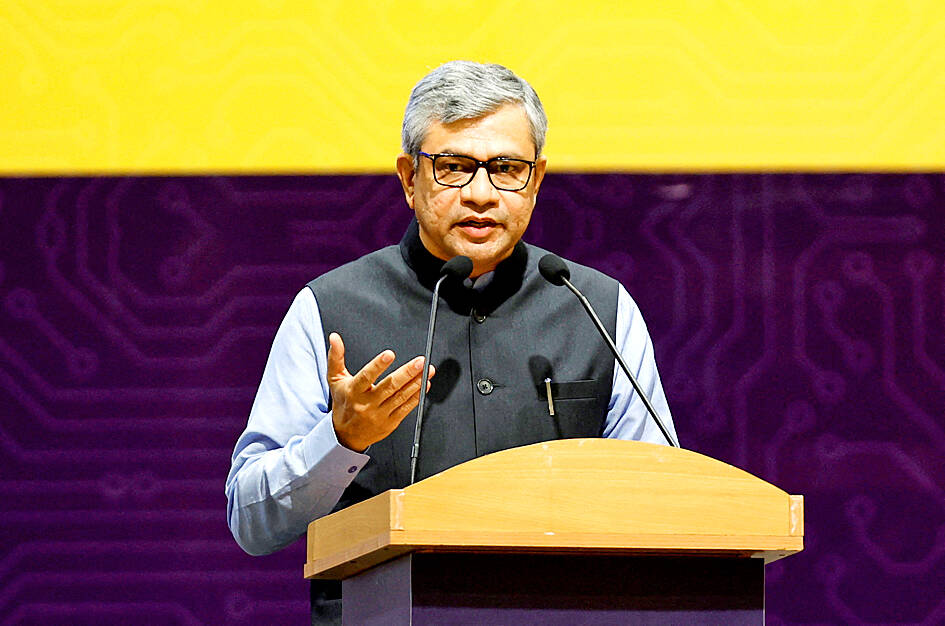
Photo: Reuters
“We will start construction of this plant within 100 days,” the minister said during the briefing, referring to Tata’s fab.
India hopes to attract chip giants to boost its domestic manufacturing sector. The government has offered to shoulder half the cost of any approved projects, up to an initial ceiling of US$10 billion. The semiconductor fund has already helped US memory maker Micron Technology Inc establish a US$2.75 billion assembly facility in Gujarat.
Taiwan’s Powerchip Semiconductor Manufacturing Corp (PSMC, 力積電) yesterday confirmed that it would assist Tata Electronics Pvt Ltd to build India’s first 12-inch wafer fab in Dholera, Gujarat.
The fab construction will begin this year, Powerchip said in a statement, adding that the new facility is expected to create more than 20,000 jobs in India.
Through the cooperation with Powerchip, Tata Electronics, a subsidiary of Tata conglomerate, plans to produce power management ICs, display driver ICs as well as microcontrollers and high-performance computing logic chips as it aims to enter the automotive, computing and data storage, wireless communications, artificial intelligence and other end markets, the Taiwanese chipmaker said.
Semiconductors have grown into a key geopolitical battleground, with the US, Japan and China investing heavily in developing domestic capabilities.
The cooperation between PSMC and Tata is “indeed timely” at this critical moment of the global restructuring of high-tech supply chain, Powerchip chairman Frank Huang (黃崇仁) said in the statement.
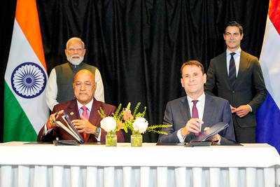
NEW MARKET: The partnership opens up India to the Dutch company, which already has a strong hold in the semiconductor market of South Korea, Taiwan and China ASML Holding NV entered into a partnership agreement with Tata Electronics Pvt Ltd aimed at ramping up India’s goal to develop domestic chip-manufacturing capabilities. The Dutch company’s technology would help power Tata Electronics’ planned 300 millimeter (mm) semiconductor foundry in Gujarat, according to a joint statement from the two companies on Saturday. The signing of a memorandum of understanding coincides with a visit by Indian Prime Minister Narendra Modi to the Netherlands, which is looking to deepen bilateral relations with New Delhi. ASML, whose top customers include Taiwan Semiconductor Manufacturing Co (台積電) and Samsung Electronics Co, makes lithography machines that can print

ROUGH RECORDS: Bonds in Japan, as well is in New Zealand, Australia and the US, are seeing the effects of a nervy market as stock exchanges across Asia edge down A deepening slump in Japanese government bonds added fuel to the selloff in global debt markets as rising oil prices stoked inflation fears and pushed yields to multi-decade highs. Japan’s 30-year yield yesterday surged as much as 20 basis points to the highest level since the tenor’s debut in 1999, before paring some of the move. Shorter-maturity Japanese debt was also under pressure, underscored by weak demand at a sale of five-year notes that offered a record-high coupon of 2 percent. Concerns over inflation and government spending rippling through markets including the US, Australia and New Zealand are being amplified in Japan,
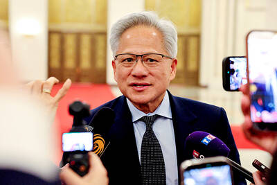
The US has cleared about 10 Chinese firms to buy Nvidia Corp’s second-most powerful artificial intelligence (AI) chip, the H200, but not a single delivery has been made so far, three people familiar with the matter said, leaving a major technology deal in limbo as chief executive officer Jensen Huang (黃仁勳) seeks a breakthrough in China this week. Huang, who was not initially listed in a White House delegation to Beijing, joined the trip after an invitation from US President Donald Trump, a source said. Trump picked him up in Alaska en route to a summit with Chinese President Xi Jinping

Wall Street is licking its chops over an unprecedented slate of massive initial public offerings (IPOs) set to arrive in the coming months, beginning with Elon Musk’s Space Exploration Technologies Corp (SpaceX) next month. That is expected to be followed by artificial intelligence (AI) rivals OpenAI and Anthropic PBC. The trio of mega listings, each eyeing valuations around US$1 trillion or more, constitutes a heady period of elevated risk and reward. SpaceX is targeting an IPO that would raise up to US$80 billion — about double the funds generated from all IPOs last year. OpenAI and Anthropic are eyeing IPOs raising US$60 billion. “We’re