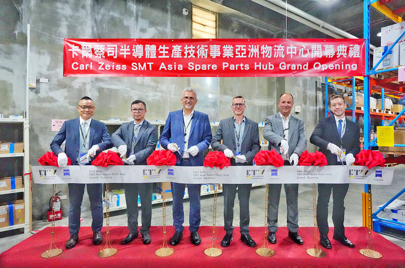
CTW Logistics and Germany’s ZEISS Semiconductor Manufacturing Technology (SMT) have announced the official inauguration of their Asian logistics center located in Taoyuan. This project partnership aims to provide more efficient supply chain services for the semiconductor industry, enhancing overall industry resilience.
The grand opening ceremony was attended by representatives from the semiconductor industry and the German Trade Office Taipei, marking a significant milestone for Taiwan’s position in the global semiconductor supply chain.
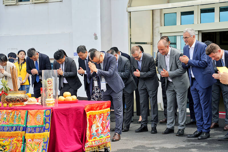
Situated in Yangmei, Taoyuan, the newly launched logistics center will offer Taiwanese and Asian customers bonded solutions, inventory management, value-added services, real-time supply chain visibility, Business Agent Scheme, and other comprehensive services. To support this hub, CTW Logistics has provided a special infrastructure for sensitive components, providing relevant value-added services within the cleanroom. In terms of sustainability, CTW Logistics has implemented digital technologies such as the Internet of Things to manage environmental variables and energy within the logistics center. They have also collaborated with Carl ZEISS to establish a modern IT infrastructure enabling real-time data exchange.
As a key logistics service provider for the semiconductor industry, CTW Logistics has accumulated extensive expertise through longstanding partnerships with global recognized manufacturers. With a service network covering the entirety of Taiwan, the company offers various critical logistics services for the semiconductor supply chain, including wafers, key components, hazardous materials, special gases, and dangerous chemicals. CTW Logistics also plans to complete the construction of the Tainan International Logistics Center in 2024, further reinforcing its service capabilities in the southern region.
During the ceremony, representatives from CTW Logistics ZEISS SMT jointly inaugurated the Asia Hub. Moving forward, the two companies will collaborate to usher in a new era for the semiconductor industry, providing customers with superior logistics support services.
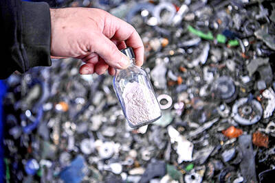
RECYCLE: Taiwan would aid manufacturers in refining rare earths from discarded appliances, which would fit the nation’s circular economy goals, minister Kung said Taiwan would work with the US and Japan on a proposed cooperation initiative in response to Beijing’s newly announced rare earth export curbs, Minister of Economic Affairs Kung Ming-hsin (龔明鑫) said yesterday. China last week announced new restrictions requiring companies to obtain export licenses if their products contain more than 0.1 percent of Chinese-origin rare earths by value. US Secretary of the Treasury Scott Bessent on Wednesday responded by saying that Beijing was “unreliable” in its rare earths exports, adding that the US would “neither be commanded, nor controlled” by China, several media outlets reported. Japanese Minister of Finance Katsunobu Kato yesterday also
Taiwan’s rapidly aging population is fueling a sharp increase in homes occupied solely by elderly people, a trend that is reshaping the nation’s housing market and social fabric, real-estate brokers said yesterday. About 850,000 residences were occupied by elderly people in the first quarter, including 655,000 that housed only one resident, the Ministry of the Interior said. The figures have nearly doubled from a decade earlier, Great Home Realty Co (大家房屋) said, as people aged 65 and older now make up 20.8 percent of the population. “The so-called silver tsunami represents more than just a demographic shift — it could fundamentally redefine the
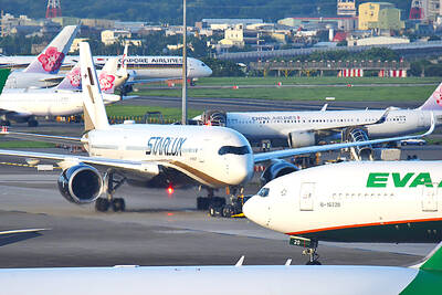
China Airlines Ltd (CAL, 中華航空) said it expects peak season effects in the fourth quarter to continue to boost demand for passenger flights and cargo services, after reporting its second-highest-ever September sales on Monday. The carrier said it posted NT$15.88 billion (US$517 million) in consolidated sales last month, trailing only September last year’s NT$16.01 billion. Last month, CAL generated NT$8.77 billion from its passenger flights and NT$5.37 billion from cargo services, it said. In the first nine months of this year, the carrier posted NT$154.93 billion in cumulative sales, up 2.62 percent from a year earlier, marking the second-highest level for the January-September
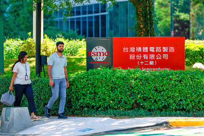
‘DRAMATIC AND POSITIVE’: AI growth would be better than it previously forecast and would stay robust even if the Chinese market became inaccessible for customers, it said Taiwan Semiconductor Manufacturing Co (TSMC, 台積電) yesterday raised its full-year revenue growth outlook after posting record profit for last quarter, despite growing market concern about an artificial intelligence (AI) bubble. The company said it expects revenue to expand about 35 percent year-on-year, driven mainly by faster-than-expected demand for leading-edge chips for AI applications. The world’s biggest contract chipmaker in July projected that revenue this year would expand about 30 percent in US dollar terms. The company also slightly hiked its capital expenditure for this year to US$40 billion to US$42 billion, compared with US$38 billion to US$42 billion it set previously. “AI demand actually