Applied Materials Inc is planning to spend as much as US$4 billion on a new research and development (R&D) center near its California headquarters, embarking on a now-rare building project in the heart of Silicon Valley.
The Equipment and Process Innovation and Commercialization (EPIC) Center on Applied Materials’ campus in Santa Clara would be the biggest R&D facility in the semiconductor industry, the company said yesterday.
Applied Materials is the largest maker of chip-manufacturing equipment, and the project would let the firm and its customers rapidly develop new production techniques.
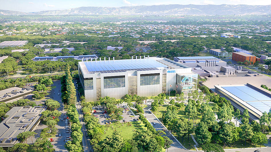
Photo: Reuters / Applied Materials Inc
Like many of the industry’s construction projects these days, the effort is also a bid to tap government funding. The US’ CHIPS and Science Act, passed last year, is to allocate roughly US$52 billion to help revitalize domestic R&D and manufacturing, and companies are angling to benefit from the windfall.
Applied Materials’ ambitions with the new center would hinge on how much assistance it gets, CEO Gary Dickerson said in an interview.
“The scale and pace of what we do is dependent on incentives,” he said.
The company chose to build in Silicon Valley — a place that has become too costly and burdensome for most new chip facilities — because of the proximity to many companies with an interest in semiconductors, he said.
Intel Corp, Nvidia Corp and Advanced Micro Devices Inc are all based in the city, about an hour’s drive south of San Francisco.
The new facility is designed to speed up improvements in the way that semiconductors are made, helping the chip business grow into a trillion-dollar market this decade.
The EPIC Center, whose name is short for equipment and process innovation and commercialization, would let chip manufacturers try out new machinery in something close to a complete production line. That should make it faster and easier to fine-tune new production technologies.
At the same time, academic institutions would have access to cutting-edge gear for research, Dickerson said.
The overall aim is to cut down on the 10 to 15 years that it takes academic research to make it to the factory floor.
The center would also help attract and train the workers that the industry needs to run plants and design chips, he said.
Dickerson said that the project is needed to help overcome daunting new technical challenges and maintain the pace of chip advancement — what he calls one of humankind’s greatest engineering achievements.
A state-of-the-art chip crams 96.5km of wiring connecting 15 billion transistors into an area that is 10 millimeters across. Some of the layers of materials deposited to create that structure are only four atoms deep.
Building the new facility would lead to an increase in Applied Materials’ capital spending over the next few years, but the company has said that its investments would not affect its ability to fund dividends and share repurchases.
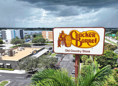
On Tuesday, US President Donald Trump weighed in on a pressing national issue: The rebranding of a restaurant chain. Last week, Cracker Barrel, a Tennessee company whose nationwide locations lean heavily on a cozy, old-timey aesthetic — “rocking chairs on the porch, a warm fire in the hearth, peg games on the table” — announced it was updating its logo. Uncle Herschel, the man who once appeared next to the letters with a barrel, was gone. It sparked ire on the right, with Donald Trump Jr leading a charge against the rebranding: “WTF is wrong with Cracker Barrel?!” Later, Trump Sr weighed
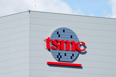
Taiwan Semiconductor Manufacturing Co (TSMC, 台積電) secured a record 70.2 percent share of the global foundry business in the second quarter, up from 67.6 percent the previous quarter, and continued widening its lead over second-placed Samsung Electronics Co, TrendForce Corp (集邦科技) said on Monday. TSMC posted US$30.24 billion in sales in the April-to-June period, up 18.5 percent from the previous quarter, driven by major smartphone customers entering their ramp-up cycle and robust demand for artificial intelligence chips, laptops and PCs, which boosted wafer shipments and average selling prices, TrendForce said in a report. Samsung’s sales also grew in the second quarter, up
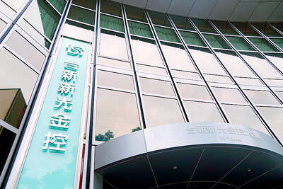
HEADWINDS: Upfront investment is unavoidable in the merger, but cost savings would materialize over time, TS Financial Holding Co president Welch Lin said TS Financial Holding Co (台新新光金控) said it would take about two years before the benefits of its merger with Shin Kong Financial Holding Co (新光金控) become evident, as the group prioritizes the consolidation of its major subsidiaries. “The group’s priority is to complete the consolidation of different subsidiaries,” Welch Lin (林維俊), president of the nation’s fourth-largest financial conglomerate by assets, told reporters during its first earnings briefing since the merger took effect on July 24. The asset management units are scheduled to merge in November, followed by life insurance in January next year and securities operations in April, Lin said. Banking integration,
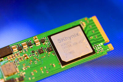
LOOPHOLES: The move is to end a break that was aiding foreign producers without any similar benefit for US manufacturers, the US Department of Commerce said US President Donald Trump’s administration would make it harder for Samsung Electronics Co and SK Hynix Inc to ship critical equipment to their chipmaking operations in China, dealing a potential blow to the companies’ production in the world’s largest semiconductor market. The US Department of Commerce in a notice published on Friday said that it was revoking waivers for Samsung and SK Hynix to use US technologies in their Chinese operations. The companies had been operating in China under regulations that allow them to import chipmaking equipment without applying for a new license each time. The move would revise what is known