Taiwan Semiconductor Manufacturing Co (TSMC, 台積電) yesterday expressed confidence that its 2-nanometer process technology would be the most advanced foundry technology in the world when it is introduced in 2025, shrugging off Samsung Electronics Co’s plans to overtake its technology leadership position.
“Today, the 3-nanometer technology we offer is the world’s most advanced technology. When we launch our 2-nanometer technology in 2025, there is no doubt in my mind that it will be the most advanced semiconductor technology in the world,” senior vice president of business development Kevin Zhang (張曉強) said in response to a reporter’s question about Samsung’s plans.
Two enhanced versions, dubbed N2P and N2X, would be launched in 2026, TSMC said during an annual technology symposium in Hsinchu.
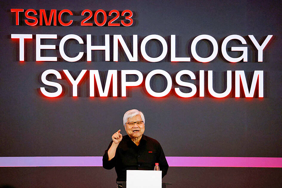
Photo: Carlos Garcia Rawlins, Reuters
Samsung aims to surpass its bigger foundry rival TSMC to become the industry leader within five years, the Korea Economic Daily reported on Thursday last week.
The South Korean technology giant expects to get ahead of TSMC with its 2-nanometer processing node, Samsung’s head of semiconductor business Kyun Kye-hyun said during a lecture.
Samsung plans to mass produce 2-nanometer chips in 2025 as well. Its 2-nanometer technology would be based on the get-all-around structure, while TSMC adopts a nano sheet transistor structure, which it believes is a more mature technology, with less power consumption and greater performance.
In preparation for the mass production of its 2-nanometer chips, TSMC, the world’s biggest contract chipmaker, is constructing a new factory in Hsinchu and would break ground for another one in Taichung next year.
The 2-nanometer chips would be used in smartphones and high-performance-computing (HPC) devices, the chipmaker said.
Commenting on market concern about TSMC’s 3-nanometer process, Zhang said the technology’s yield would soon catch up with that of its 5-nanometer process.
“We have strong confidence in our 3-nanometer processor, which is stable,” Zhang said. “We are seeing 1.5 to two times the number of customers engaging in our 3-nanometer [technology] compared with 5-nanometer during the initial period.”
Its automaker customers are participating in a program to upgrade to a new version of 3-nanometer auto chips, called Auto Early technology, Zhang said.
The new technology would allow customers to start designing chips two to three years earlier than before and to shorten their time to market, he said.
TSMC last month said that it was unable to meet customers’ demand for 3-nanometer chips.
Most of its smartphone and HPC customers are migrating to the 3-nanometer technology, Zhang said.
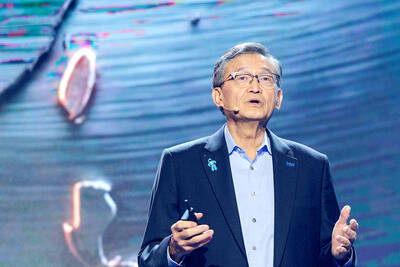
TSMC chief executive officer C.C. Wei (魏哲家) yesterday in Hsinchu said that TSMC is a more reliable and trustworthy partner, as it does not compete with its customers.
“Our two competitors, one from South Korea and one based in California, develop their [own] products,” Wei said.
“TSMC does not develop [its own] products. We do not compete with you,” he told customers.
Samsung and Intel Corp are competing with TSMC to vie for a bigger market share and technology leadership.
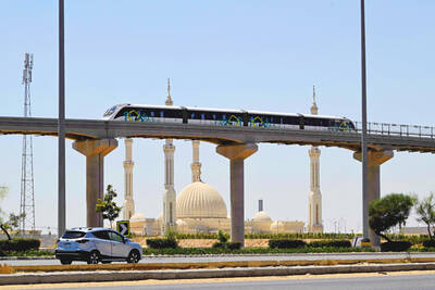
Cairo’s new monorail slices across the city skyline, running above the familiar chaos of blaring horns and aging buses’ exhaust fumes that mark rush hour below. The US$4.5 billion monorail, opened this month, is among Egypt’s most prominent new transport projects, part of a debt-funded infrastructure drive criticized for sapping state finances while bringing limited benefits to most of the country’s 109 million people. “It feels like you’re in a different country,” said Ramy Sayed, a restaurant manager, aboard a driverless Innovia 300 train. “No noise, no traffic, we’re not used to this.” The eastern line runs 56km from the bustling middle-class

Taiwanese firms have increased investment in the Philippines in recent years as Manila’s ties with Washington deepen and global supply chains continue to shift away from China, an expert at the Chung-Hua Institution for Economic Research (CIER, 中華經濟研究院) said yesterday. The Philippines had not been among Taiwanese investors’ top choices in Southeast Asia, CIER Taiwan ASEAN Studies Center director Kristy Hsu (徐遵慈) said at a seminar in Taipei. However, Taiwan’s investment in the country has grown significantly since the COVID-19 pandemic, reaching US $257 million last year, a high in recent years, she said. Although Taiwan’s total investment in the Philippines still lags
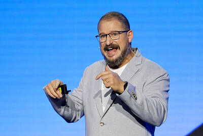
Intel Corp regards Taiwan Semiconductor Manufacturing Co (TSMC, 台積電) as a longstanding partner, as the US chipmaker would continue outsourcing production of advanced chips to TSMC, Intel chief executive officer Lip-Bu Tan (陳立武) said yesterday. “I don’t look at people as competitors. I look at the collaboration... Nvidia is also, you know, a good friend,” Tan told a news conference following his keynote speech at the Computex trade show in Taipei. “It’s a very trusted partnership for us... We are a big, top customer for them, and we’re going to continue doing that,” he said, referring to TSMC, the world’s largest foundry
Artificial intelligence (AI) agents would supplant smartphones as the center of people’s digital lives, fundamentally reshaping personal devices and driving a major computing upgrade cycle, Qualcomm Inc CEO Cristiano Amon said yesterday. In his keynote speech for this year’s Computex trade show in Taipei, Amon said that the rise of "agentic AI" — AI systems capable of reasoning, planning and carrying out tasks autonomously — would transform how people interact with technology across phones, PCs, vehicles and wearable devices. Describing the technology as the next major evolution in computing, Amon said that "2026 is the year of agents.” For decades, smartphones have sat