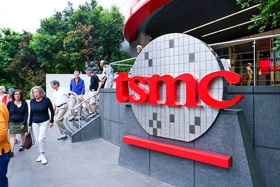
Taiwan Semiconductor Manufacturing Co (TSMC, 台積電) on Saturday said that it would hold a ceremony on Thursday to mark the beginning of mass production using its 3-nanometer process.
The company is to mark the placing of the final beam at its Fab 18 in the Southern Taiwan Science Park (南部科學園區) in Tainan.
It would also detail its plans for expanding 3-nanometer production at the facility in the coming years, TSMC said.
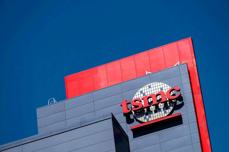
Photo: Lam Yik Fei, Bloomberg
The fab currently mass produces chips using the 5-nanometer process.
It is unusual for TSMC to hold a ceremony to mark the beginning of commercial production of a new technology.
Analysts have said that the ceremony aims to announce TSMC’s intention to continue using Taiwan as a hub for research and development (R&D) and production, despite its overseas investments.
Speculation has risen that the company could relocate its production and R&D centers to the US.
The rumors arose after TSMC on Dec. 6 said at a tool-in ceremony for its 12-inch wafer plant in Phoenix, Arizona, that it would increase its planned US$12 billion investment there to US$40 billion to build a 3-nanometer fab by 2026, in addition to its planned 4-nanometer plant due to be completed in 2024.
The concerns intensified after TSMC sent a large group of Taiwanese engineers to support the Arizona plant, raising investors’ fears that the move could undermine the firm’s base in Taiwan.
The planned Arizona plants are expected to produce more than 600,000 wafers a year, TSMC has said.
Last week, TSMC chief executive officer C.C. Wei (魏哲家) told a forum held by the Mount Jade Global Science and Technology Association in Taipei that there was “no chance” that a single wafer fab would give a location a technical advantage over other semiconductor manufacturing sites.
TSMC plans to start mass producing chips using the N3E process next year. The process is based on the 3-nanometer technology and produces more efficient chips with a better yield rate.
The company is also developing a more sophisticated 2-nanometer process and plans to build a 2-nanometer fab in Hsinchu, with mass production scheduled to begin in 2025.
The 3-nanometer process uses 16-nanometer fin field-effect transistor technology, which is a 3D transistor structure that allows a chip to run faster using the same amount of energy or to run at the same speed on reduced power.
Chips made using the technology are 10 to 15 percent faster and 25 to 30 percent more energy-efficient than those produced with the 5-nanometer process, whose mass production started last year.
Apple Inc and Intel Corp are expected to place orders for chips made with TSMC’s 3-nanometer process, analysts have said.
The 2-nanometer process would be the first technology in which TSMC employs a gate-all-around structure, which reduces undesirable variability and mobility loss, making the technology the most competitive and efficient on the market, the company has said.
Early this month, Wayne Wang (王永壯), director general of the Hsinchu Science Park Bureau, said TSMC has plans to build a 1-nanometer process fab in the Longtan (龍潭) section of the Hsinchu Science Park (新竹科學園區).
TSMC has yet to confirm Wang’s announcement.

Cairo’s new monorail slices across the city skyline, running above the familiar chaos of blaring horns and aging buses’ exhaust fumes that mark rush hour below. The US$4.5 billion monorail, opened this month, is among Egypt’s most prominent new transport projects, part of a debt-funded infrastructure drive criticized for sapping state finances while bringing limited benefits to most of the country’s 109 million people. “It feels like you’re in a different country,” said Ramy Sayed, a restaurant manager, aboard a driverless Innovia 300 train. “No noise, no traffic, we’re not used to this.” The eastern line runs 56km from the bustling middle-class
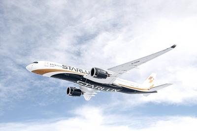
Starlux Airlines Co (星宇航空) today unveiled a long-haul network expansion plan at a shareholders’ meeting in Taipei, including direct flights to Barcelona, Spain, and Zurich, Switzerland, as well as a service connecting Taipei, Sydney and New Zealand. Starlux is to become the first Taiwanese carrier to offer non-stop services to the two European cities, while the inaugural oceanic route is expected to expand transit opportunities within the Australia-New Zealand market, Starlux said. Flight services to Chicago, Dallas, Washington and New York are under evaluation, the airline added. Prior to the shareholders’ meeting, the airline earlier this year announced that it would be
Taiwanese prosecutors suspect that three people successfully smuggled at least one shipment of Nvidia Corp artificial intelligence (AI) chips to China after first exporting them to Japan, people familiar with the matter said. The trio was detained last week by the Keelung District Prosecutors’ Office for allegedly falsifying documents related to exports of Super Micro Computer Inc servers containing advanced Nvidia chips, which the US has barred from sale to China without a license from Washington. The move marked Taiwan’s first public crackdown on AI chip diversion after years of pressure from the US to take a more active role in curtailing
Taiwan Semiconductor Manufacturing Co (TSMC, 台積電) employee bonuses are likely to grow more than 30 percent this year, in line with the past few years as the company’s profits continue to set new records, an anonymous source cited TSMC chairman C.C. Wei (魏哲家) as saying yesterday. TSMC, the world’s largest contract chipmaker, is committed to taking care of its workers, the source said, citing Wei’s meeting with employees yesterday morning. Wei also expressed gratitude to employees for their contribution to the company’s improving bottom line, the source added. Since 2023, TSMC’s employee bonuses have grown at an annual rate of