Toshiba Corp is to build a new 300mm wafer fabrication plant for power semiconductors that would more than double its production capacity by March 2025, the company said yesterday.
Construction of the new facility in Japan’s Ishikawa Prefecture would take place in two phases, the company said.
When the first phase is fully operational, Toshiba’s power semiconductor capacity would be 2.5 times greater than in fiscal 2021.
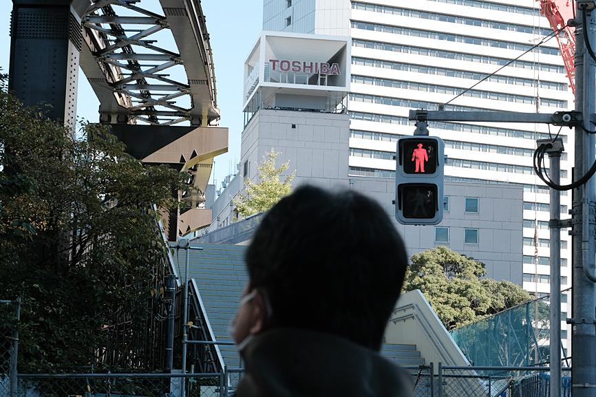
Photo: Bloomberg
Toshiba would invest about ¥100 billion (US$870 million) to build the facility, the Nikkei newspaper reported earlier.
The move comes as auto and electronics makers struggle to procure even basic chips for routine tasks such as power management and wireless connectivity.
TDK Corp last month warned that shortages of components are unlikely to abate for the rest of this year, while console makers Sony Group Corp and Nintendo Co this week said that they expect semiconductor and shipping challenges to persist.
Vehicle electrification and the automation of industrial equipment are two major trends driving up demand for power-regulating chips, Toshiba said in its statement.
It is targeting 100 percent reliance on renewable energy for the fab, it said.
Toshiba in September last year said it was struggling to fulfill orders because of shortages of materials and output capacity.
Despite investor concern that demand would evaporate after the frenzy for electronics fueled by the COVID-19 pandemic, the company is confident that orders would keep growing rapidly enough to sell out all its production lines for years to come.
Toshiba is due to brief investors on its business strategies next week as it tussles with activist shareholders over the future of the company.
The company in November last year said that it plans to split into three firms as a way to create value for shareholders, but one major stock holder has publicly questioned the plan, while another leading investor has called on Toshiba to rebuild trust with shareholders after years of scandals and corporate governance issues.
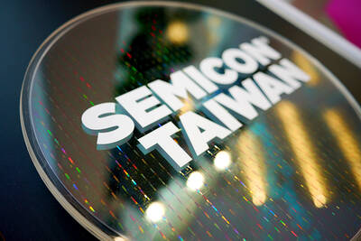
With this year’s Semicon Taiwan trade show set to kick off on Wednesday, market attention has turned to the mass production of advanced packaging technologies and capacity expansion in Taiwan and the US. With traditional scaling reaching physical limits, heterogeneous integration and packaging technologies have emerged as key solutions. Surging demand for artificial intelligence (AI), high-performance computing (HPC) and high-bandwidth memory (HBM) chips has put technologies such as chip-on-wafer-on-substrate (CoWoS), integrated fan-out (InFO), system on integrated chips (SoIC), 3D IC and fan-out panel-level packaging (FOPLP) at the center of semiconductor innovation, making them a major focus at this year’s trade show, according
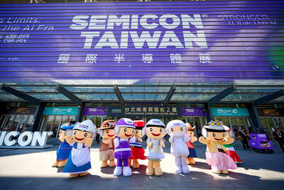
DEBUT: The trade show is to feature 17 national pavilions, a new high for the event, including from Canada, Costa Rica, Lithuania, Sweden and Vietnam for the first time The Semicon Taiwan trade show, which opens on Wednesday, is expected to see a new high in the number of exhibitors and visitors from around the world, said its organizer, SEMI, which has described the annual event as the “Olympics of the semiconductor industry.” SEMI, which represents companies in the electronics manufacturing and design supply chain, and touts the annual exhibition as the most influential semiconductor trade show in the world, said more than 1,200 enterprises from 56 countries are to showcase their innovations across more than 4,100 booths, and that the event could attract 100,000 visitors. This year’s event features 17
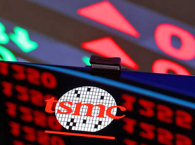
SEMICONDUCTOR SERVICES: A company executive said that Taiwanese firms must think about how to participate in global supply chains and lift their competitiveness Taiwan Semiconductor Manufacturing Co (TSMC, 台積電) yesterday said it expects to launch its first multifunctional service center in Pingtung County in the middle of 2027, in a bid to foster a resilient high-tech facility construction ecosystem. TSMC broached the idea of creating a center two or three years ago when it started building new manufacturing capacity in the US and Japan, the company said. The center, dubbed an “ecosystem park,” would assist local manufacturing facility construction partners to upgrade their capabilities and secure more deals from other global chipmakers such as Intel Corp, Micron Technology Inc and Infineon Technologies AG, TSMC said. It
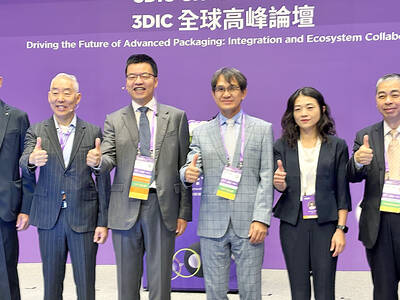
EXPORT GROWTH: The AI boom has shortened chip cycles to just one year, putting pressure on chipmakers to accelerate development and expand packaging capacity Developing a localized supply chain for advanced packaging equipment is critical for keeping pace with customers’ increasingly shrinking time-to-market cycles for new artificial intelligence (AI) chips, Taiwan Semiconductor Manufacturing Co (TSMC, 台積電) said yesterday. Spurred on by the AI revolution, customers are accelerating product upgrades to nearly every year, compared with the two to three-year development cadence in the past, TSMC vice president of advanced packaging technology and service Jun He (何軍) said at a 3D IC Global Summit organized by SEMI in Taipei. These shortened cycles put heavy pressure on chipmakers, as the entire process — from chip design to mass