Japanese technology and entertainment giant Sony has bought Hawk-Eye, the British-based firm whose computer systems assist umpires and track the path of balls in sports such as tennis and cricket.
The two firms did not disclose the value of the transaction, but the Nikkei newspaper estimated it to be worth “several billion yen.”
Sony will use Hawk-Eye’s know-how, technology and business network in the sports industry to improve its sports-related products, such as IT solutions for sports arenas, the company said in a statement dated Monday.
“Hawk-Eye presents Sony with the opportunity to acquire a small, innovative company with unique knowledge and excellent growth and synergies potential,” Naomi Climer, vice-president of Sony Europe, said in the statement.
The deal will complement Sony’s existing business portfolio for sports professionals, such as IT solutions for stadiums, venues and broadcasters, Climer said.
Sony is a major sponsor of many sports events and offers a full line of equipment for sports media professionals.
Hawk-Eye was launched in 1999 and its technology has helped transform global sports coverage on TV to become the reference standard for ball tracking and graphics in sports such as tennis, cricket and snooker.
It can be used to provide instant graphic replays that help determine whether the ball was in or out during tennis matches or inform key umpire decisions in cricket.
“Our skills and established knowledge coupled with Sony’s breadth of capabilities and technologies will create immense opportunities for the sports industry,” Paul Hawkins, founder of Hawk-Eye, said in the statement.
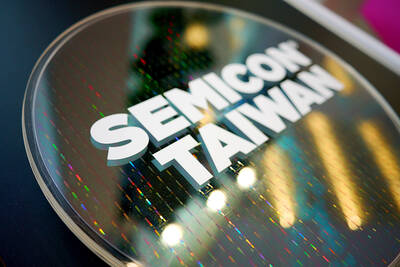
With this year’s Semicon Taiwan trade show set to kick off on Wednesday, market attention has turned to the mass production of advanced packaging technologies and capacity expansion in Taiwan and the US. With traditional scaling reaching physical limits, heterogeneous integration and packaging technologies have emerged as key solutions. Surging demand for artificial intelligence (AI), high-performance computing (HPC) and high-bandwidth memory (HBM) chips has put technologies such as chip-on-wafer-on-substrate (CoWoS), integrated fan-out (InFO), system on integrated chips (SoIC), 3D IC and fan-out panel-level packaging (FOPLP) at the center of semiconductor innovation, making them a major focus at this year’s trade show, according
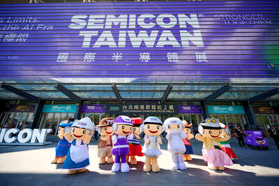
DEBUT: The trade show is to feature 17 national pavilions, a new high for the event, including from Canada, Costa Rica, Lithuania, Sweden and Vietnam for the first time The Semicon Taiwan trade show, which opens on Wednesday, is expected to see a new high in the number of exhibitors and visitors from around the world, said its organizer, SEMI, which has described the annual event as the “Olympics of the semiconductor industry.” SEMI, which represents companies in the electronics manufacturing and design supply chain, and touts the annual exhibition as the most influential semiconductor trade show in the world, said more than 1,200 enterprises from 56 countries are to showcase their innovations across more than 4,100 booths, and that the event could attract 100,000 visitors. This year’s event features 17
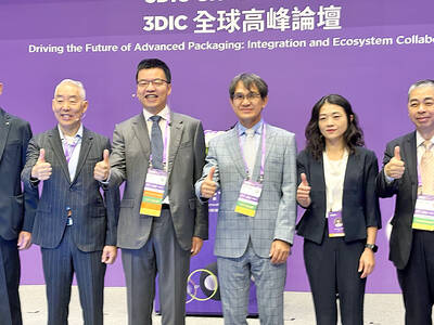
EXPORT GROWTH: The AI boom has shortened chip cycles to just one year, putting pressure on chipmakers to accelerate development and expand packaging capacity Developing a localized supply chain for advanced packaging equipment is critical for keeping pace with customers’ increasingly shrinking time-to-market cycles for new artificial intelligence (AI) chips, Taiwan Semiconductor Manufacturing Co (TSMC, 台積電) said yesterday. Spurred on by the AI revolution, customers are accelerating product upgrades to nearly every year, compared with the two to three-year development cadence in the past, TSMC vice president of advanced packaging technology and service Jun He (何軍) said at a 3D IC Global Summit organized by SEMI in Taipei. These shortened cycles put heavy pressure on chipmakers, as the entire process — from chip design to mass
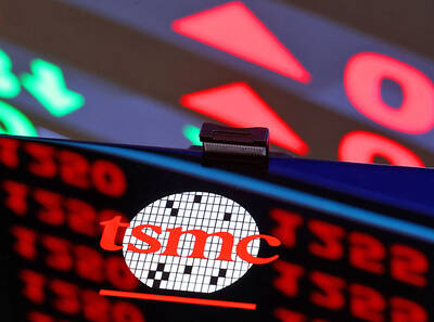
SEMICONDUCTOR SERVICES: A company executive said that Taiwanese firms must think about how to participate in global supply chains and lift their competitiveness Taiwan Semiconductor Manufacturing Co (TSMC, 台積電) yesterday said it expects to launch its first multifunctional service center in Pingtung County in the middle of 2027, in a bid to foster a resilient high-tech facility construction ecosystem. TSMC broached the idea of creating a center two or three years ago when it started building new manufacturing capacity in the US and Japan, the company said. The center, dubbed an “ecosystem park,” would assist local manufacturing facility construction partners to upgrade their capabilities and secure more deals from other global chipmakers such as Intel Corp, Micron Technology Inc and Infineon Technologies AG, TSMC said. It