US computer chip giant Intel announced plans on Friday to invest more than US$5 billion to build a new state-of-the-art chip manufacturing facility in Arizona.
The announcement was made by Intel president and chief executive Paul Otellini during a visit by US President Barack Obama to an Intel facility in Hillsboro, Oregon.
Intel, the world’s largest computer chip maker, said construction of the new facility, Fab 42, in Chandler, Arizona, will begin in the middle of this year and it is expected to be completed in 2013.
“When completed, Fab 42 will be the most advanced high--volume semiconductor factory in the world,” Otellini said.
Intel said the new Arizona factory will make transistors with a minimum size of 14 nanometers.
“Building the new fab on the leading-edge 14-nanometer process enables Intel to manufacture more powerful and efficient computer chips,” Intel said in a statement.
A nanometer is one-billionth of a meter or one ninety-thousandth the width of a human hair.
“The investment positions our manufacturing network for future growth,” said Brian Krzanich, senior vice president and general manager for manufacturing and supply chain at Intel.
“The products based on these leading-edge chips will give consumers unprecedented levels of performance and power efficiency across a range of computing devices from high-end servers to ultra-sleek portable devices,” Krzanich said.
Intel announced plans in October to invest between US$6 billion and US$8 billion in its domestic manufacturing facilities to produce next-generation computer chips, including building a new fabrication plant in Oregon.
Obama traveled to Intel’s most sophisticated semiconductor plant in Oregon to tout his plans to invest in science and education despite seeking ways to rein in spending in other areas to deal with a ballooning deficit.
Obama also named Otellini to his jobs council on Friday in a move designed to harness the power of innovation to ignite economic and employment growth.
Otellini will serve on the president’s Council on Jobs and Competitiveness, an advisory board, headed by General Electric chief executive Jeffrey Immelt and dedicated to finding new ways to boost growth, hiring and the education and training of US workers.

MAJOR BENEFICIARY: The company benefits from TSMC’s advanced packaging scarcity, given robust demand for Nvidia AI chips, analysts said ASE Technology Holding Co (ASE, 日月光投控), the world’s biggest chip packaging and testing service provider, yesterday said it is raising its equipment capital expenditure budget by 10 percent this year to expand leading-edge and advanced packing and testing capacity amid strong artificial intelligence (AI) and high-performance computing chip demand. This is on top of the 40 to 50 percent annual increase in its capital spending budget to more than the US$1.7 billion to announced in February. About half of the equipment capital expenditure would be spent on leading-edge and advanced packaging and testing technology, the company said. ASE is considered by analysts

TRANSFORMATION: Taiwan is now home to the largest Google hardware research and development center outside of the US, thanks to the nation’s economic policies President Tsai Ing-wen (蔡英文) yesterday attended an event marking the opening of Google’s second hardware research and development (R&D) office in Taiwan, which was held at New Taipei City’s Banciao District (板橋). This signals Taiwan’s transformation into the world’s largest Google hardware research and development center outside of the US, validating the nation’s economic policy in the past eight years, she said. The “five plus two” innovative industries policy, “six core strategic industries” initiative and infrastructure projects have grown the national industry and established resilient supply chains that withstood the COVID-19 pandemic, Tsai said. Taiwan has improved investment conditions of the domestic economy
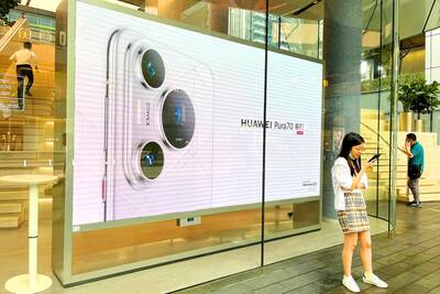
Huawei Technologies Co’s (華為) latest smartphones carry a version of the advanced made-in-China processor it revealed last year, results from an independent analysis showed. This underscored the Chinese company’s ability to sustain production of the controversial chip. The Pura 70 series unveiled last week sports the Kirin 9010 processor, research firm TechInsights found during a teardown of the device. This is a newer version of the Kirin 9000s, made by Semiconductor Manufacturing International Corp (SMIC, 中芯) for the Mate 60 Pro, which had alarmed officials in Washington who thought a 7-nanometer chip was beyond China’s capabilities. Huawei has enjoyed a resurgence since

purpose: Tesla’s CEO sought to meet senior Chinese officials to discuss the rollout of its ‘full self-driving’ software in China and approval to transfer data they had collected Tesla Inc CEO Elon Musk arrived in Beijing yesterday on an unannounced visit, where he is expected to meet senior officials to discuss the rollout of "full self-driving" (FSD) software and permission to transfer data overseas, according to a person with knowledge of the matter. Chinese state media reported that he met Premier Li Qiang (李強) in Beijing, during which Li told Musk that Tesla's development in China could be regarded as a successful example of US-China economic and trade cooperation. Musk confirmed his meeting with the premier yesterday with a post on social media platform X. "Honored to meet with Premier Li