A leading notebook computer manufacturer yesterday questioned the results of a recent study showing that some notebook computers emit an excessively high level of electromagnetic waves during wireless Internet connection.
An official from Acer, who requested anonymity, said that the company's portable computers had passed the safety guidelines for use in a wireless environment.
The Acer official's remarks came in the wake of the Taiwan Environmental Protection Union's (
The tests found that the electromagnetic emissions generated by 14 of the products exceeded 2,000 microwatts per square meter during wireless Internet connection -- much higher than the safety level of 1 microwatt set by Austria for indoor spaces.
The 14 models were manufactured by different brands, including FIC (
The Acer official said that National Taiwan University staff had carried out similar tests on the campus after the release of the union's findings.
The tests showed that the electromagnetic emissions were below 1 microwatt, which is within the safety level, the official said.
Chang Sheng (
The company is the contractor for the Wifly project, whose wireless Internet service covers most of Taipei.
"Studies show that electromagnetic waves emitted by wireless notebooks are weaker than those of handsets," he said.
Chen Shu-hua (
However, their electromagnetic emissions were very low during a wired Internet connection, Chen said.
Saying that electromagnetic waves in indoor spaces tend to exceed the safe level if two or more computers are using wireless networking at the same time, Chen warned that indoor wireless connection should not be encouraged in places such as classrooms, libraries and crowded spaces.
The union urged relevant government agencies to require computer manufacturers to label the electromagnetic emission levels of their products in order to protect consumers.
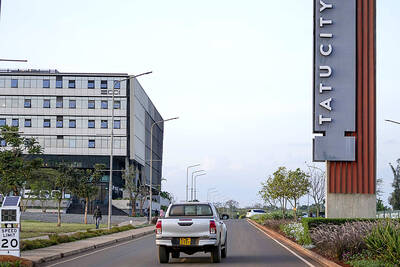
To many, Tatu City on the outskirts of Nairobi looks like a success. The first city entirely built by a private company to be operational in east Africa, with about 25,000 people living and working there, it accounts for about two-thirds of all foreign investment in Kenya. Its low-tax status has attracted more than 100 businesses including Heineken, coffee brand Dormans, and the biggest call-center and cold-chain transport firms in the region. However, to some local politicians, Tatu City has looked more like a target for extortion. A parade of governors have demanded land worth millions of dollars in exchange

An Indonesian animated movie is smashing regional box office records and could be set for wider success as it prepares to open beyond the Southeast Asian archipelago’s silver screens. Jumbo — a film based on the adventures of main character, Don, a large orphaned Indonesian boy facing bullying at school — last month became the highest-grossing Southeast Asian animated film, raking in more than US$8 million. Released at the end of March to coincide with the Eid holidays after the Islamic fasting month of Ramadan, the movie has hit 8 million ticket sales, the third-highest in Indonesian cinema history, Film
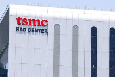
BIG BUCKS: Chairman Wei is expected to receive NT$34.12 million on a proposed NT$5 cash dividend plan, while the National Development Fund would get NT$8.27 billion Taiwan Semiconductor Manufacturing Co (TSMC, 台積電), the world’s largest contract chipmaker, yesterday announced that its board of directors approved US$15.25 billion in capital appropriations for long-term expansion to meet growing demand. The funds are to be used for installing advanced technology and packaging capacity, expanding mature and specialty technology, and constructing fabs with facility systems, TSMC said in a statement. The board also approved a proposal to distribute a NT$5 cash dividend per share, based on first-quarter earnings per share of NT$13.94, it said. That surpasses the NT$4.50 dividend for the fourth quarter of last year. TSMC has said that while it is eager
‘IMMENSE SWAY’: The top 50 companies, based on market cap, shape everything from technology to consumer trends, advisory firm Visual Capitalist said Taiwan Semiconductor Manufacturing Co (TSMC, 台積電) was ranked the 10th-most valuable company globally this year, market information advisory firm Visual Capitalist said. TSMC sat on a market cap of about US$915 billion as of Monday last week, making it the 10th-most valuable company in the world and No. 1 in Asia, the publisher said in its “50 Most Valuable Companies in the World” list. Visual Capitalist described TSMC as the world’s largest dedicated semiconductor foundry operator that rolls out chips for major tech names such as US consumer electronics brand Apple Inc, and artificial intelligence (AI) chip designers Nvidia Corp and Advanced