Taiwan Semiconductor Manufac-turing Co's (TSMC, 台積電) is moving forward with the hottest technology and proving why it is the number one semiconductor "foundry" in the world, with over 50 percent market share in this business. A semiconductor foundry manufactures microchips to the specifications of design firms, who paint a picture of the "perfect" chip, then ask TSMC to actually make it.
One of the factors that has separated TSMC from the rest of the pack is how fast it moves up the ladder to new manufacturing process technologies. Since last year, the firm has been engaged in the use of two new technologies at the same time, 12-inch silicon wafers, upon which semiconductor transistors are carved at a microscopic 0.13 microns. The "old" technology is 8-inch silicon wafers and 0.18 micron technology.
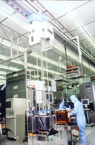
PHOTO: CHIANG YING-YING, TAIPEI TIMES
The new 12-inch wafer Fab is in the Tainan Science-Based Industrial Park (台南科學園區), and as Charles Hung (洪錦輝), the program manager on the new line puts it, some of the changes that need to be made in the manufacturing line are giving him a "a very big headache."
"In the past, we increased the wafer size in small leaps, from 3-inch to 4-inch, 5-inch, 6-inch, then from 6-inch to 8-inch. But this time, the jump is really big, from 8 to 12. It is a ridiculous jump, so there are a lot of challenges," said Hung.
The company agreed to dress this reporter up in "clean room fatigues" and offer a tour of the new Fab -- "no photographs, please" -- and a chance to learn how to make a semiconductor from a 12-inch silicon wafer.
Semiconductors are made on round, flat pieces of silicon, currently the size and shape of a round dinner plate (12-inches). Why these plates are called silicon "wafers" is a mystery. Large, round plates that look like steel and feel about as heavy -- there is nothing wafer-like about them to the touch.
Since microchips are square -- each 12-inch wafer has hundreds of thousands of square semiconductors carved onto its surface before the wafer is sent to another company for cutting and packaging, the obvious first question was: "Why is a silicon wafer round when microchips are square?"
"That's the way silicon is made," explained Hung.
Silicon wafers are produced by crystallizing highly purified silicon in a cylinder-shaped container. Afterwards, the tube-shaped silicon is sliced like bread, and polished. These slices, called wafers, are cut to a precise thickness and are uniformly flat.
"Another advantage of [12-inch] wafers is the size ... because it is bigger so the curve is closer to a square," said Hung, "So it is more efficient."
A typical microchip is about the size of your fingernail and, nearly invisible to the human eye, millions of transistors and diodes dot its surface. The transistors and diodes are arranged in precise patterns and are joined together by layers of interconnecting metal. The design of the chip determines its function and how fast it will process electronic signals.
Neat freaks
To get on to the manufacturing floor of the 12-inch facility, all employees start at the clean room, where they don uniforms for the day, a full white suit, boots and mask that cover every part of the body except the eyes. Then employees walk across a long, sticky black mat to clean off the bottoms of their boots.
And the tidiness doesn't stop there. To make sure the chips are clean throughout the process each silicon wafer is loaded into a clear, see-through box, called a pod, with 25 wafers in each. This pod is used to transport the wafers through the entire manufacturing process, protecting them from any stray dust or particles as it passes through each stage. Once the pod is attached to a new machine, a robotic arm inside the machine handles each wafer, eliminating human touch all together.
The changeover to 12-inch wafers has caused problems, though, as a pod of 8-inch wafers only weighed five kilograms, whereas the new 12-inch wafers weigh in at a whopping 9kg per pod.
The new size and weight of wafers at the 12-inch plant has forced TSMC to experiment with its equipment in order to achieve the same productivity as 8-inch plants enjoy. The company is also using more robotic equipment to carry the pods through each step in the manufacturing process, since the wafers inside are getting too bulky.
Cost of production
One major headache Hung has been trying to tackle in the pilot line is getting the cost of production to equal, then surpass that of the older technology, 8-inch silicon wafers.
"Is the cost equal? No, right now, the cost is not equal," said Tsai Nun-sian (
The major issue is speed, getting a heavier silicon wafer through the equipment at the same rate or faster than an 8-inch wafer.
On an 8-inch wafer, it usually it takes 30 days from start to finish to get through the entire manufacturing process. And Tsai says TSMC won't be able to achieve this kind of speed in 12-inch wafers until late next year. Of course, in the transition to the new technology, this was anticipated.
The pilot line is a learning tool for the company and a place to try out equipment made by different semiconductor tool manufacturers.
"Once we select the right equipment, we continue to work with the supplier and help upgrade the performance of the tools," said Tsai.
So to make a semiconductor, one of the first steps in the process is to polish the 12-inch wafers and prepare it for photographing. Long before this step, however, a "mask" must be made.
The semiconductor design (also called an IC or integrated circuit design) must be carved into a "mask" made of quartz crystal. This quartz crystal mask will then be placed on top of each 12-inch wafer inside an ion imprinting machine, where the quartz crystal mask shows the ion imprinter where to paint the semiconductor design. Although "painting" is the term used in this article, it is more like exposing a photograph. Exposure chemicals are used and the wafer has to go through a developing process.
After imprinting the design, as the silicon wafer is passed along the manufacturing process, the design is already on the wafer and other machines actually carve out the semiconductor design.
"The mask defines the circuit pattern, that is all that needs to be changed to run the design of a new company through the process," said Hung, explaining how designs are changed quickly in a semiconductor foundry.
When changing to a new technology, companies like TSMC depend on semiconductor equipment makers to create user-friendly machines. Sometimes, the vendor will simply make the equipment bigger to accommodate the new size of the wafer, in this case 12 inches. Other firms will redesign tools and software and the customer has to decide which company to buy from.
With a half dozen semiconductor equipment vendors to choose from, the 12-inch pilot line helps the company experiment with which tools fit its needs best.
"For certain machines our experienced engineers will use their expertise, and based on their experience they will say whether a design is good or not, but it is still difficult to tell" without testing, said Hung.
Next, the wafers undergo the Wafer Acceptance Test, and if they pass the test, they are considered good wafers and pass through to additional processes. TSMC, however, plays no part in the next stage of making a semiconductor.
The round wafer with hundreds of thousands of semiconductors etched into it is then sent on to another company like Advanced Semiconductor Engineering Inc (ASE,
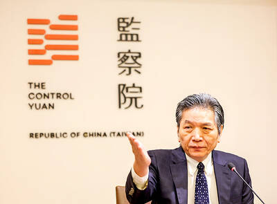
‘ABUSE OF POWER’: Lee Chun-yi allegedly used a Control Yuan vehicle to transport his dog to a pet grooming salon and take his wife to restaurants, media reports said Control Yuan Secretary-General Lee Chun-yi (李俊俋) resigned on Sunday night, admitting that he had misused a government vehicle, as reported by the media. Control Yuan Vice President Lee Hung-chun (李鴻鈞) yesterday apologized to the public over the issue. The watchdog body would follow up on similar accusations made by the Chinese Nationalist Party (KMT) and would investigate the alleged misuse of government vehicles by three other Control Yuan members: Su Li-chiung (蘇麗瓊), Lin Yu-jung (林郁容) and Wang Jung-chang (王榮璋), Lee Hung-chun said. Lee Chun-yi in a statement apologized for using a Control Yuan vehicle to transport his dog to a
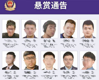
Taiwan yesterday denied Chinese allegations that its military was behind a cyberattack on a technology company in Guangzhou, after city authorities issued warrants for 20 suspects. The Guangzhou Municipal Public Security Bureau earlier yesterday issued warrants for 20 people it identified as members of the Information, Communications and Electronic Force Command (ICEFCOM). The bureau alleged they were behind a May 20 cyberattack targeting the backend system of a self-service facility at the company. “ICEFCOM, under Taiwan’s ruling Democratic Progressive Party, directed the illegal attack,” the warrant says. The bureau placed a bounty of 10,000 yuan (US$1,392) on each of the 20 people named in
The High Court yesterday found a New Taipei City woman guilty of charges related to helping Beijing secure surrender agreements from military service members. Lee Huei-hsin (李慧馨) was sentenced to six years and eight months in prison for breaching the National Security Act (國家安全法), making illegal compacts with government employees and bribery, the court said. The verdict is final. Lee, the manager of a temple in the city’s Lujhou District (蘆洲), was accused of arranging for eight service members to make surrender pledges to the Chinese People’s Liberation Army in exchange for money, the court said. The pledges, which required them to provide identification

INDO-PACIFIC REGION: Royal Navy ships exercise the right of freedom of navigation, including in the Taiwan Strait and South China Sea, the UK’s Tony Radakin told a summit Freedom of navigation in the Indo-Pacific region is as important as it is in the English Channel, British Chief of the Defence Staff Admiral Tony Radakin said at a summit in Singapore on Saturday. The remark came as the British Royal Navy’s flagship aircraft carrier, the HMS Prince of Wales, is on an eight-month deployment to the Indo-Pacific region as head of an international carrier strike group. “Upholding the UN Convention on the Law of the Sea, and with it, the principles of the freedom of navigation, in this part of the world matters to us just as it matters in the