Flat-panel display maker Innolux Corp (群創) yesterday said it is stepping up investment on developing panel-level packaging technologies, and that it plans to allocate more than 15 percent of its capital expenditures next year to the new semiconductor business.
This investment demonstrates Innolux’s determination to diversify from a pure flat-panel display manufacturer and to escape from the industry’s boom-and-bust cycles, the Miaoli-based company said.
The chip packaging business would play a vital role in the company’s transformation efforts, it said.
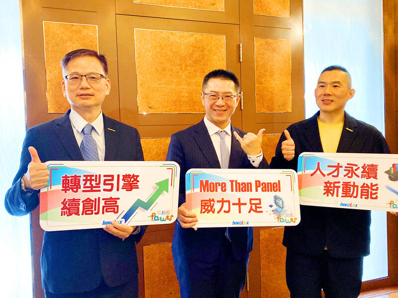
Photo: Lisa Wang, Taipei Times
This year, Innolux planned to spend about 15 percent of its annual capital expenditures, about NT$20 billion (US$612 million) or a little under that amount, on semiconductor-related technologies and equipment. About 85 percent would be allocated for its core display business, it said.
“In the long term, we hope for the semiconductor and display businesses to each account for half of the company’s total expenditures,” Innolux chairman Jim Hung (洪進揚) told reporters during an annual media event in Taipei yesterday.
“We intend to raise the portion of semiconductor investment each year,” Hung said.
Innolux’s entry into the semiconductor packaging sector has caught the attention of investors and semiconductor experts, as advanced packaging technologies are seen as potential solutions to extending Moore’s Law, when scaling technology reaches its physical limits. This is a reference to Intel co-founder Gordon Moore, who observed in 1965 that the number of transistors on an integrated circuit were doubling about every two years with minimal rise in cost.
Innolux’s aim is to create a new value-added business by leveraging its flat-panel display capacity and technologies. The first step is to revitalize a less advanced 3.5-generation flat panel fab and repurpose the glass substrates for chip packaging to create better value, since the fab is not cost-competitive, the company said.
The company originally planned to start shipping the first products using its first-generation panel level package (PLP) technology, called Chip-First technology, by the end of this year, it said, adding that it was targeting mid-to-low-end chips such as power ICs, or radio-frequency ICs, which are mostly used in smartphones and other consumer electronics.
However, a slump in smartphone demand stalled the company’s plan, Hung said.
Now, the company hopes to postpone the shipment until the first half of next year, when smartphone demand picks up a bit, he said.
Despite the setback, Innolux continues investing in second and third-generation PLP technologies, with the aim of progressing to mid-range and advanced chips.
To tap into silicon photonics, a new chip packaging technology, Innolux has acquired unspecified shares of two small-scale companies, BE Epitaxy Semiconductor Technology Co Ltd (元澄半導體科技) and Best Epitaxy Manufacturing Co Ltd (先發光電), it said.
Hung said that he had reached his turn-around goal for the company during his first 6-year tenure.
Innolux reported its second profitable quarter in a row, with profits of NT$421 million last quarter. In the first three quarters of this year, it accumulated losses of NT$2.55 billion, an improvement from losses of NT$15.4 billion during the same period last year.
Local rival AUO Corp (友達) has been in the red for the last 10 quarters. Losses have improved to NT$4.68 billion during the first three quarters, compared with losses of NT$16.69 billion a year ago.

Taiwanese firms have increased investment in the Philippines in recent years as Manila’s ties with Washington deepen and global supply chains continue to shift away from China, an expert at the Chung-Hua Institution for Economic Research (CIER, 中華經濟研究院) said yesterday. The Philippines had not been among Taiwanese investors’ top choices in Southeast Asia, CIER Taiwan ASEAN Studies Center director Kristy Hsu (徐遵慈) said at a seminar in Taipei. However, Taiwan’s investment in the country has grown significantly since the COVID-19 pandemic, reaching US $257 million last year, a high in recent years, she said. Although Taiwan’s total investment in the Philippines still lags
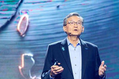
Intel Corp regards Taiwan Semiconductor Manufacturing Co (TSMC, 台積電) as a longstanding partner, as the US chipmaker would continue outsourcing production of advanced chips to TSMC, Intel chief executive officer Lip-Bu Tan (陳立武) said yesterday. “I don’t look at people as competitors. I look at the collaboration... Nvidia is also, you know, a good friend,” Tan told a news conference following his keynote speech at the Computex trade show in Taipei. “It’s a very trusted partnership for us... We are a big, top customer for them, and we’re going to continue doing that,” he said, referring to TSMC, the world’s largest foundry
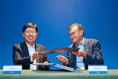
Hon Hai Precision Industry Co (鴻海精密) yesterday said it would work with US chipmaker Intel Corp to jointly develop and deploy next-generation artificial intelligence (AI) infrastructure and intelligent computing platforms in a move to capture booming demand for AI computing systems. Hon Hai, also known as Foxconn Technology Group (富士康), said in a statement that the partnership would combine its global manufacturing scale, system integration expertise and AI data center deployment capabilities with Intel’s strengths in processor architecture, silicon technologies and software ecosystem. The companies said they plan to work on equipment used in AI data centers, including server racks powered by
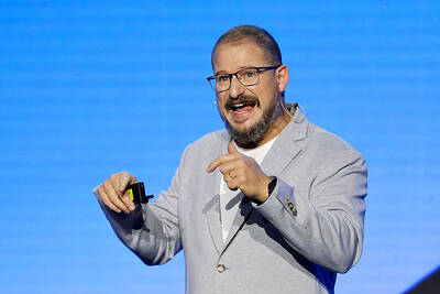
Artificial intelligence (AI) agents would supplant smartphones as the center of people’s digital lives, fundamentally reshaping personal devices and driving a major computing upgrade cycle, Qualcomm Inc CEO Cristiano Amon said yesterday. In his keynote speech for this year’s Computex trade show in Taipei, Amon said that the rise of "agentic AI" — AI systems capable of reasoning, planning and carrying out tasks autonomously — would transform how people interact with technology across phones, PCs, vehicles and wearable devices. Describing the technology as the next major evolution in computing, Amon said that "2026 is the year of agents.” For decades, smartphones have sat