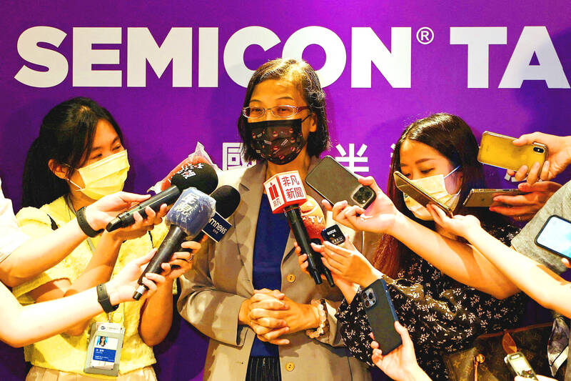
GlobalWafers Co (環球晶圓), the world’s No. 3 silicon wafer supplier, yesterday said it secured up to US$400 million in direct funding from the US Department of Commerce under the CHIPS and Science Act for the construction of two new advanced fabs in the US.
Its subsidiaries GlobalWafers America and MEMC LLC are to build a 12-inch silicon wafer fab in Sherman, Texas, and another one in Missouri to produce silicon-on-insulator (SOI) wafers used to make leading-edge chips.
“With the support of the [US President Joe] Biden Administration, we are honored to be bringing to American shores the world’s most cutting-edge 12-inch semiconductor wafer technology, filling what the White House has called a ‘key vulnerability’ within the US semiconductor supply chain,” GlobalWafers America president Mark England said in a statement.

Photo: Ann Wang, Reuters
“GlobalWafers is fully committed to the US market, and we are excited to be playing a defining role in the nation’s semiconductor rebirth,” England said.
When completed, the Texas complex would be the first 12-inch silicon wafer fab built in the US in more than 20 years, he said.
The Texas facility is on track to ramp up volume production in the first quarter of next year, GlobalWafers said.
The new fabs would play a critical role in enhancing the resilience of US semiconductor supply chains, as they would supply US chip designers with domestic wafer capacity to make leading-edge chips for artificial-intelligence (AI) applications or to produce silicon photonics devices used in next-generation packaging technology, GlobalWafers said.
GlobalWafers would reduce the US’ complete dependence on overseas manufacturing facilities, the company said.
The planned 12-inch SOI facility in Missouri would be the first 12-inch fab based in the state when it is completed, the company said.
MEMC is operates an 8-inch SOI fab in Missouri.
The US government funding would be “greatly helpful” in elevating competitiveness of its US fabs, GlobalWafers chairwoman Doris Hsu (徐秀蘭) told a virtual media briefing yesterday, adding that US manufacturing costs tend to be much higher than in Taiwan.
The US$400 million grant would account for about 10 percent of the company’s overall investments of less than US$4.8 billion, Hsu said.
In addition to the direct grant announced yesterday, GlobalWafers plans to apply for the US Department of Treasury’s Advanced Manufacturing Investment Credit of up to 25 percent of qualified expenditures of its subsidiaries, Hsu said.
The US federal funding would comprise one-third of the company’s investments in the two US fabs, Hsu said.
GlobalWafers has secured long-term supply agreements from US customers, including GlobalFoundries Inc, to fill about 80 percent of its planned capacities at the Texas and Missouri facilities, Hsu said.

The domestic unit of the Chinese-owned, Dutch-headquartered chipmaker Nexperia BV will soon be able to produce semiconductors locally within China, according to two company sources. Nexperia is at the center of a global tug-of-war over critical semiconductor technology, with a Dutch court in February ordering a probe into alleged mismanagement at the company. The geopolitical tussle has disrupted supply chains, with some carmakers reportedly forced to cut production due to chip shortages. Local production would allow Nexperia’s domestic arm, Nexperia Semiconductors (China) Ltd (安世半導體中國), to bypass restrictions in place since October on the supply of silicon wafers — etched with tiny components to

Singapore-based ride-hailing and delivery giant Grab Holdings Ltd has applied for regulatory approval to acquire the Taiwan operations of Germany-based Delivery Hero SE's Foodpanda in a deal valued at about US$600 million. Grab submitted the filing to the Fair Trade Commission on Friday last week, with the transaction subject to regulatory review and approval, the company said in a statement yesterday. Its independent governance structure would help foster a healthy and competitive market in Taiwan if the deal is approved, Grab said. Grab, which is listed on the NASDAQ, said in the filing that US-based Uber Technologies Inc holds about 13 percent of

Taiwan Semiconductor Manufacturing Co (TSMC, 台積電) yesterday received government approval to deploy its advanced 3-nanometer (3nm) process at its second fab currently under construction in Japan, the Ministry of Economic Affairs said in a news release. The ministry green-lit the plan for the facility in Kumamoto, which is scheduled to start installing equipment and come online in 2028 with a monthly production capacity of 15,000 12-inch wafers, the ministry said. The Department of Investment Review in June 2024 authorized a US$5.26 billion investment for the facility, slated to manufacture 6- to 12nm chips, significantly less advanced than 3nm process. At a meeting with

Taiwan’s food delivery market could undergo a major shift if Singapore-based Grab Holdings Ltd completes its planned acquisition of Delivery Hero SE’s Foodpanda business in Taiwan, industry experts said. Grab on Monday last week announced it would acquire Foodpanda’s Taiwan operations for US$600 million. The deal is expected to be finalized in the second half of this year, with Grab aiming to complete user migration to its platform by the first half of next year. A duopoly between Uber Eats and Foodpanda dominates Taiwan’s delivery market, a structure that has remained intact since the Fair Trade Commission (FTC) blocked Uber Technologies Inc’s