They call it “the shrink” — it is the challenge of how to pack more circuits onto the microchips that power everything from our smartphones to our computers, even our coffee machines.
Pushing the boundaries of this technology is Dutch company ASML Holding NV, which since its foundation in 1984 has quietly become a world leader in the semiconductor business.
“There is more power in your smartphone today than was used to put man on the moon,” said ASML chief operating officer Frederic Schneider-Maunoury, animatedly waving his mobile phone in the air.
When you open an app on your smartphone, the chain allowing you to book a flight, message a friend or check out who is hot in your neighborhood most likely arcs all the way back to ASML.
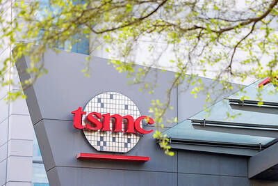
Headquartered in Veldhoven, near the Belgian border, it builds sophisticated lithography machines to enable the world’s top chipmakers — Intel Corp, Samsung Electronics Co and Apple Inc supplier Taiwan Semiconductor Manufacturing Co (台積電) — to produce the smallest, most powerful and most cost-effective microprocessors on the planet.
Its newest machines use highly focused extreme ultra-violet (EUV) light to imprint designs on the chips, and are at the cutting edge of what is technologically possible in the art of miniaturization.
Last year, after two decades of research and development and billions of euros, ASML shipped its first 12 EUV machines to clients. Each costs about 120 million euros (US$143.53 million). This year, it has projected sales of 20 machines — by 2020, it hopes to be selling 35 to 40 a year.
It is ironic that these machines, which produce chips of infinitesimally small dimensions, are the size of a bus. Three Boeing 747 aircraft are needed to transport one machine to a client.
Long seen as a bellwether of the tech industry, the company is listed on the Amsterdam bourse, the AEX and the NASDAQ in New York.
Last year it announced profits had almost doubled to 2.12 billion euros on record sales of 9.05 billion euros.
Only two other companies in the world — the Japanese giants Nikon Corp and Canon Corp — make lithography machines and neither has yet developed EUV technology.
“Our problem is not just to find the technologies, we have to put it into the products in an economical way,” Schneider-Maunoury told reporters at his office.
ASML now employs about 20,000 people, mostly engineers and most in Veldhoven, but it also has sites in Asia and the US.
As it grows, it is hiring. About 3,000 new posts were added last year, with a similar number of new jobs expected this year.

Shares of contract chipmaker Taiwan Semiconductor Manufacturing Co (TSMC, 台積電) came under pressure yesterday after a report that Apple Inc is looking to shift some orders from the Taiwanese company to Intel Corp. TSMC shares fell NT$55, or 2.4 percent, to close at NT$2,235 on the local main board, Taiwan Stock Exchange data showed. Despite the losses, TSMC is expected to continue to benefit from sound fundamentals, as it maintains a lead over its peers in high-end process development, analysts said. “The selling was a knee-jerk reaction to an Intel-Apple report over the weekend,” Mega International Investment Services Corp (兆豐國際投顧) analyst Alex Huang
Taiwan Semiconductor Manufacturing Co (TSMC, 台積電) is expected to remain Apple Inc’s primary chip manufacturing partner despite reports that Apple could shift some orders to Intel Corp, industry experts said yesterday. The comments came after The Wall Street Journal reported on Friday that Apple and Intel had reached a preliminary agreement following more than a year of negotiations for Intel to manufacture some chips for Apple devices. Taiwan Institute of Economic Research (台灣經濟研究院) economist Arisa Liu (劉佩真) said TSMC’s advanced packaging technologies, including integrated fan-out and chip-on-wafer-on-substrate, remain critical to the performance of Apple’s A-series and M-series chips. She said Intel and Samsung
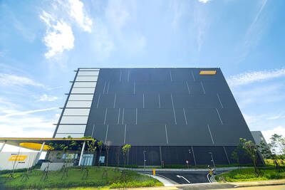
POWER BUILDUP: Powered by Nvidia’s B200 Blackwell chips, the data center would support MediaTek’s computing power demand and business growth, the company said Smartphone chip designer MediaTek Inc (聯發科) yesterday launched a new artificial intelligence (AI) data center with a maximum capacity of 45 megawatts to meet its rising demand for computing power required to develop new advanced chips for AI applications. The company has completed the first-phase computing power buildup at the data center in Miaoli County’s Tongluo Township (銅鑼), providing 15 megawatts of capacity to support its research and development (R&D) capabilities, despite an industrywide shortage of key components, MediaTek said. Supply constraints have plagued a wide range of key components, including memory chips, solid-state drives, power supply units and central
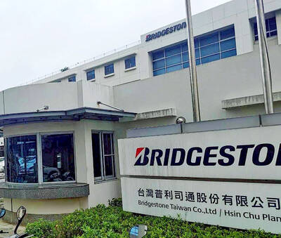
TRANSITION: With the closure, the company would reorganize its Taiwanese unit to a sales and service-focused model, Bridgestone said Bridgestone Corp yesterday announced it would cease manufacturing operations at its tire plant in Hsinchu County’s Hukou Township (湖口), affecting more than 500 workers. Bridgestone Taiwan Co (台灣普利司通) said in a statement that the decision was based on the Tokyo-based tire maker’s adjustments to its global operational strategy and long-term market development considerations. The Taiwanese unit would be reorganized as part of the closure, effective yesterday, and all related production activities would be concluded, the statement said. Under the plan, Bridgestone would continue to deepen its presence in the Taiwanese market, while transitioning to a sales and service-focused business model, it added. The Hsinchu