Taiwan Semiconductor Manufacturing Co (TSMC, 台積電), the world’s largest contract chipmaker, yesterday said the Internet of Things (IoT) would be the industry’s major growth driver in the next three to five years.
The uptake of the IoT, including wearable devices, would spur demand for key components such as microcontrollers, image sensors and Wi-Fi and Bluetooth sensors, said John Wei (尉濟時), a senior director of TSMC’s mobile and computing business division.
“Those components will not entirely be made at 8-inch factories. Many of them, such as Wi-Fi and Bluetooth [sensors], are produced at 12-inch factories… The demand will be diverse from low-end [chips] to high-end [chips],” Wei told reporters on the sidelines of a press conference for the annual SEMICON exhibition in Taipei.
Wei said the IoT would not represent significant shipments in the near term, but it would be a big growth engine for the semiconductor industry in next three to five years, when the whole ecosystem and business model matured.
TSMC would be ready with the technologies needed, from power management ICs to application processors, he said.
Wei’s comments echoed TSMC chairman Morris Chang’s (張忠謀) speech on the “Next Big Thing” in March, when he said the IoT would be the industry’s new growth driver, taking over mobile devices such as smartphones and tablets.
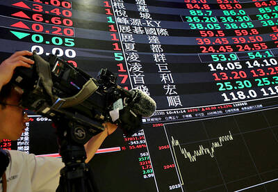
SEMI Taiwan president Terry Tsao (曹世綸) yesterday said that the global semiconductor equipment market is expected to expand at a rate of 20.8 percent this year to US$38.4 billion and would grow about 11 percent year-on-year to US$42.6 billion next year, with Taiwan being the top consumer.
Tsao attributed the growth to new investment in IoT technologies.
Separately, equipment maker ASML Holding NV said its customers using advanced extreme ultraviolet (EUV) lithography would mass produce wafers by the end of 2016.
“We have made some progress. And we believe the EUV system will allow our customers to save manufacturing costs effectively,” ASML Taiwan director of technical marketing Peter Cheng (鄭國偉) said on the sidelines of the SEMICON press conference.
“More than one customer have had their EUV lithography machines reach a throughput of 500 wafers per day,” Cheng said.
The daily throughput is expected to increase to 15,000 wafers a day by 2016, based on the company’s roadmap, Cheng said.
Early last month, ASML confirmed that IBM Corp marked an EUV throughput record by producing 637 wafers a day.
EUV is the leading candidate for printing fine patterns for next-generation chips.
TSMC was not certain whether it would start using the EUV system to manufacture chips on 10-nanometer (nm) or 7-nanometer process technologies. TSMC is scheduled to start mass production of 10nm chips in 2017.
SEMI Taiwan said the annual trade show has attracted 650 companies around the world to showcase their latest products at the three-day exhibition, up from last year’s 586 companies.
Shanghai Integrated Circuit Industry Association consultant Xue Zi (薛自) said 13 of its members, including semiconductor equipment supplier North Microelectronics (北方微電子), would attend the show.
The number has doubled from last year, when the association’s members joined the show for the first time, Xue said.
After several years flying high as Asia’s best Nvidia Corp proxy, Taiwan Semiconductor Manufacturing Co (TSMC, 台積電) is increasingly vying with other artificial intelligence (AI) stocks for investor attention. Stock traders are chasing a wider array of beneficiaries as mainstream usage of AI creates demand for hardware beyond the most-advanced chips TSMC makes for Nvidia. Subthemes from the deepening memory crunch to advances in robotics are also luring bids. At the same time, investment caps on single stocks are pushing funds to diversify, while retail investors long familiar with TSMC through its US depositary receipts are being offered a broader set of
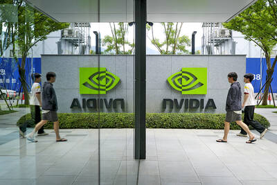
UNDER MICROSCOPE: Taiwan detained three people who allegedly conspired to buy servers in Taiwan and export them using fraudulent documentation, prosecutors said Nvidia Corp chief executive officer Jensen Huang (黃仁勳) on Saturday urged Super Micro Computer Inc to tighten up on compliance after Taiwan detained three people this week for allegedly making fraudulent declarations about artificial intelligence (AI) servers made by its US partner. The development marked the nation’s first crackdown on semiconductor smuggling, which grew after the US slapped restrictions on exports of high-end chips such as Nvidia AI accelerators to China. Nvidia is “rigorous” in explaining regulations to all of its partners, Huang told reporters after arriving in Taipei. “Ultimately Super Micro has to run their own company,” he said in response to
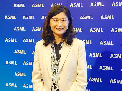
Netherlands-based semiconductor equipment supplier ASML Holding NV yesterday said that it is planning to hire an additional 1,000 people in Taiwan this year in response to growing demand from clients. ASML had previously planned to recruit 600 people this year, but that the plan has been adjusted upward, ASML vice president and ASML Taiwan general manager Grace Wang (汪佳慧) told reporters. ASML has a workforce of more than 4,500 in Taiwan, accounting for about 10 percent of its global total, Wang said. This year’s recruitment campaign would focus on adding people in the customer support, manufacturing and supply chain domains to assist ASML
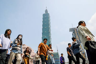
TECH RELIANCE: Growth is increasingly reflecting an unequal K-shaped distribution, where technology sectors outperform and other industries struggle, an expert said Standard Chartered Bank has significantly raised its forecast for Taiwan’s economic growth to 9.5 percent this year, up from 7.6 percent previously, citing surging artificial intelligence (AI) demand driving exports, semiconductor production and investment. The upgrade reflects a sustained AI supercycle that continues to fuel demand for advanced chips and technology infrastructure, which form the backbone of Taiwan’s exports, the bank said in a report this week. “We raise our 2026 growth forecast to reflect a much stronger-than-expected first-quarter GDP figure,” Standard Chartered senior economist for greater China and Asia Tommy Wu (胡東安) said in the report. Driven largely by a 35.3 percent