AU Optronics Corp (AUO, 友達光電) has suspended production at a plant, which makes polysilicon used in solar wafer manufacturing, in Japan and is assessing potential quake damage to supply chains in the LCD panel industry, the company said.
The Hsinchu-based company said in a statement on Saturday that its manufacturing facilities had not been damaged and there had been no casualties at its Japanese solar-wafer unit, M.Setek Co, in Fukushima Prefecture, one of the areas hardest hit by the magnitude 8.9 earthquake on Friday.
M.Setek produces polysilicon and solar wafers in Soma City, Fukushima Prefecture, both of which are key raw materials for making solar cells. AUO has in recent years expanded into the solar power business, aiming to gain a foothold in the fast-growing green energy market.
AUO has about 800 employees in Japan, with about 700 working at M.Setek, chairman Lee Kun-yao (李焜耀) said yesterday on the sidelines of a job fair in Taipei.
“The [M.Setek] plant was not hit by the tsunami, but ... because of a lack of water and electricity, it is not operational at the moment,” local cable TV network UBN quoted Lee as saying yesterday.
The company downplayed the potential financial impact from the production suspension, adding that M.Setek contributed just 0.3 percent of AUO’s NT$102.62 billion consolidated revenue in the fourth quarter of last year.
As for the possible knock-on effect on the LCD panel industry, Lee said there would certainly be an impact in terms of the upstream supply chain, but that an accurate assessment would require more time.
“We have alternative sources of chemical materials,” Lee said, hinting that the earthquake has had a limited impact on the company’s flat-panel business.
US market researcher IHS iSuppli said on Friday that the earthquake would affect the production of components for LCD panels — including glass, color filters, polarizers, cold cathode fluorescent lamps and light-emitting diodes — as Japanese suppliers play an important role in this line of business.
Meanwhile, Lee said yesterday the company would re-apply to the Investment Commission for permission to change its Chinese investment plan, after the government announced on March 8 that it would allow Taiwanese LCD makers to buy a stake in or merge with Chinese counterparts, as well as invest in Chinese fabs using the same level of technology they currently employ in Taiwan.
In December, the company won government approval to invest US$3 billion in a 7.5-generation fab in Kunshan, China.
ADDITIONAL REPORTING BY CHEN MEI-YING
Taichung reported the steepest fall in completed home prices among the six special municipalities in the first quarter of this year, data compiled by Taiwan Realty Co (台灣房屋) showed yesterday. From January through last month, the average transaction price for completed homes in Taichung fell 8 percent from a year earlier to NT$299,000 (US$9,483) per ping (3.3m²), said Taiwan Realty, which compiled the data based on the government’s price registration platform. The decline could be attributed to many home buyers choosing relatively affordable used homes to live in themselves, instead of newly built homes in the city’s prime property market, Taiwan Realty
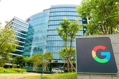
The government yesterday approved applications by Alphabet Inc’s Google to invest NT$27.08 billion (US$859.98 million) in Taiwan, the Ministry of Economic Affairs said in a statement. The Department of Investment Review approved two investments proposed by Google, with much of the funds to be used for data processing and electronic information supply services, as well as inventory procurement businesses in the semiconductor field, the ministry said. It marks the second consecutive year that Google has applied to increase its investment in Taiwan. Google plans to infuse NT$25.34 billion into Charter Investments Ltd (特許投資顧問) through its Singapore-based subsidiary Fructan Holdings Singapore Pte Ltd, and

JET JUICE: The war on Iran’s secondary effects have seen fuel prices skyrocket, knocking flight schedules down to earth in return as airlines struggle with costs Airline passengers should brace for more irritation in the next few months as carriers worldwide cancel flights and ground planes to cope with stratospheric increases in jet-fuel prices. Dutch flag carrier KLM is the latest company to cut its schedule, saying on Thursday that it would scrap 80 return flights at Amsterdam’s Schiphol Airport in the coming month. That puts it in the same league as United Airlines Holdings Inc, Deutsche Lufthansa AG and Cathay Pacific Airways Ltd, which have all pruned itineraries to mitigate costs. Global capacity for next month has been reduced by about 3 percentage points, with all

The US said it plans to help build a first-of-its-kind industrial hub in the Philippines to boost production of inputs crucial to US supply chains. The 4,000-acre hub is intended to be “a purpose-built platform for allied manufacturing” and “an investment acceleration hub where the specific industrial activities are shaped by market demand,” the US Department of State said on Thursday. The project — touted as an “economic security zone” — would be within the Luzon Economic Corridor, a flagship economic project backed by the US and Japan on the main Philippine island. The project was also described as “the first artificial intelligence